
Through Part 5 we wrote the rules into the code one at a time, and this round the numbers got considerably better.
| Item | Right after routing | After cleanup |
|---|---|---|
| Right-angle (90°) bends | 28 | 3 |
| Arbitrary-angle segments | 78 (132mm) | 17 |
| Nets with mixed widths | 16 | 0 |
| DRC violations | 13 | 12 |
Three techniques did the work.
1. Step the chamfer size down. The old tool only ever tried one chamfer size. Where the space is tight, DRC blocks it and that corner stays a right angle forever. Stepping down 0.8 → 0.5 → 0.35 → 0.25 … resolved half of them.
2. Cut the batch from 15 to 3. The loop is “apply → DRC → roll back if worse,” done in batches, and a large batch lets one bad edit kill 14 good ones along with it. With batches of 15, only 7 of 97 survived; with batches of 3, 50 of 66 did.
3. Push the junction along the neighbor’s axis. A trace that drifts slightly off straight — 2.19°, for instance — can be corrected by pushing its junction along the axis of an adjacent trace, provided that neighbor is axis-aligned. The neighbor keeps its angle and only changes length, and the offending trace lands on an exact angle. This resolved 44 of 62.
Zooming in on the routing — four problems
Routing quality looked settled because the numbers were better. Then we zoomed way in on the routing.
- Vias sit out in open space with long traces trailing from them. No human would put a via there.
- Bottom-layer traces cross over top-side pads repeatedly. Different layers, so DRC passes, but it violates the rule about not running between component pads.
- Parallel bundles are packed at minimum spacing, with no room left to widen the gaps.
- Detours that climb and come back down diagonally are still sitting there.
The measurements had already been saying it. 12.9 bends per net on average. Detour ratio up to 3.0× — 224mm of trace to make a 74mm connection. We had just kept applying polish on top of that.
Reducing the number of rule violations and improving the routing are two different things.
Three right angles and 17 arbitrary-angle segments is “able to pass the gates,” not “able to be released as a production drawing.”
The cause was a shortage of copper layers
The copper layer count was the answer, and the measurements at the end of Part 5 already held it. The 4-channel IO board — the production board in the same family — is 4-layer, and its two inner layers are not ground planes but real routing layers.
| Board | Top | Inner 2 | Inner 3 | Bottom |
|---|---|---|---|---|
| 4-channel IO (production) | 369mm | 344mm | 262mm | 439mm |
We were cramming a 16-channel board — four times the channels — onto two layers.
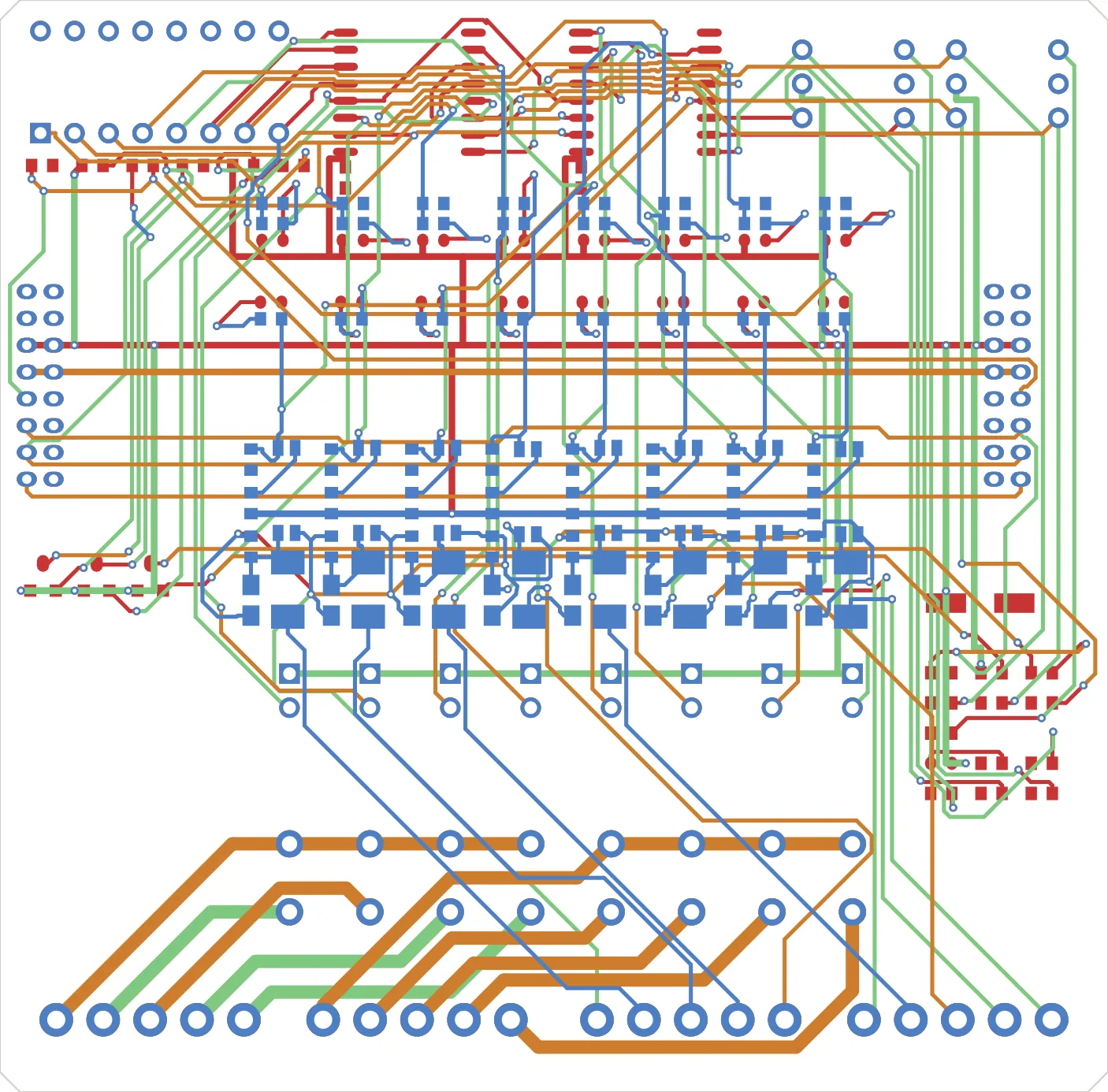
The finished routing with a different color per layer, overlaid. Red and orange are the two outer layers, green and blue the two inner ones. Much of what Part 4 was forcing onto two layers now runs on the inner layers — which is precisely how much room opened up for straight vertical and horizontal runs.
With no space, the router responds the only way it can: 0.06mm jog segments to squeeze past, vias dropped anywhere to change layers, crossings over pads. And trying to clean that up in post-processing runs straight into DRC. When we tried to absorb the tiny segments, only 7 of 97 went through; the rest caused clearance violations the moment they were applied. Those segments existed precisely because there was no space there.
Moving to four layers through the KiCad API
KiCad layer numbers are not something to guess at; we changed them through the API. Writing them directly gets the numbering wrong (in KiCad 10 it is F.Cu=0, B.Cu=2, In1.Cu=4, In2.Cu=6 — not consecutive).
b = pcbnew.LoadBoard("io16.kicad_pcb")
b.SetCopperLayerCount(4)
pcbnew.SaveBoard("io16.kicad_pcb", b)
Then we re-injected the per-layer directions for four layers. Part 4 injected top = horizontal and bottom = vertical into the DSN, but the layer names were hard-coded for a 2-layer board, so the inner layers were getting no direction at all. We changed it to read the layer names from the board and alternate.
| Layer | Direction |
|---|---|
| F.Cu | Horizontal |
| In1.Cu | Vertical |
| In2.Cu | Horizontal |
| B.Cu | Vertical |
(The dot in In1.Cu is a regex metacharacter. Forget to escape it and it silently fails
to match.)
What we learned — metrics are not routing quality
The most expensive lesson of this round is this.
Do not confuse fixing a quality metric with making the product good.
Right-angle counts, angle distribution, and width uniformity are all necessary conditions. You can satisfy every one of them and still have bad routing. And when those conditions keep refusing to be met, that may not mean the post-processing is inadequate — it may mean it was impossible in that space to begin with.
When the numbers refuse to improve, the question to ask before writing one more post-processing tool is whether this board is even big enough to hold this circuit.
Reducing rule violations and improving the routing are two different things, and conditions that keep refusing to be met are a sign that the board is short on layers.
Part 7 — The war on the last one: the hardest part of automation is the end — a full account of the issues that surfaced right before the finish line
Earlier in this series: Part 1, Part 2, Part 3, Part 4, and Part 5 on the measurement changing the board.
Contact
- Email: [email protected]
- Instagram: https://www.instagram.com/going.sen/
- Website: https://intosen.com/kr/consult/
Comments
Enter a nickname to leave a comment, or sign in with Google or GitHub.