
Part 11 was a 118 × 125 mm board. This one is the small side of the same project: 88 × 90 mm, two layers, 39 parts. It half-wave rectifies 220 V into the electromagnet of a motor brake and watches whether current is actually flowing in the coil, returning a single signal point to the controller above it.
Every gate was green.
DRC            0 violations · 0 unrouted · 0 schematic parity errors
Isolation      0 violations
Creepage/clearance  3,514 pairs · 0 below spec · 4 exceptions (pins inside a package)
Routing        178 segments, 813.0 mm · 26 vias
So we said “the board is finished, all that is left is placing the order.” Six things came out after we said it, and three of them were holes in the very checks that let us say “finished.”
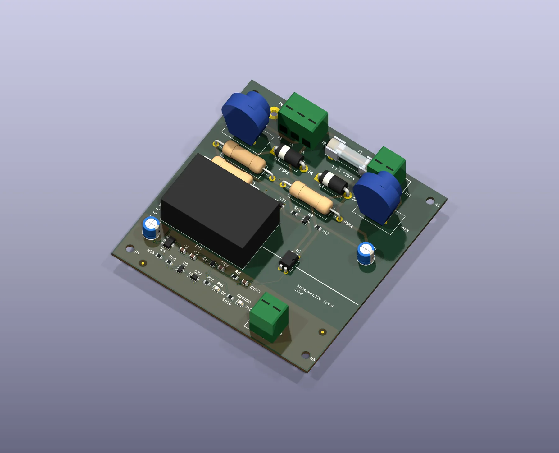
The finished board. The mains area at the top carries the rectifier and the larger parts; the monitoring circuit sits in the low-voltage area below.
The isolation barrier - trace width is the voltage difference
One picture before the rest. Below is the 2D artwork. The yellow line running across the middle is the boundary between mains (above) and SELV (below). The thick traces above are 1.0 mm; the thin ones below are 0.25 mm.
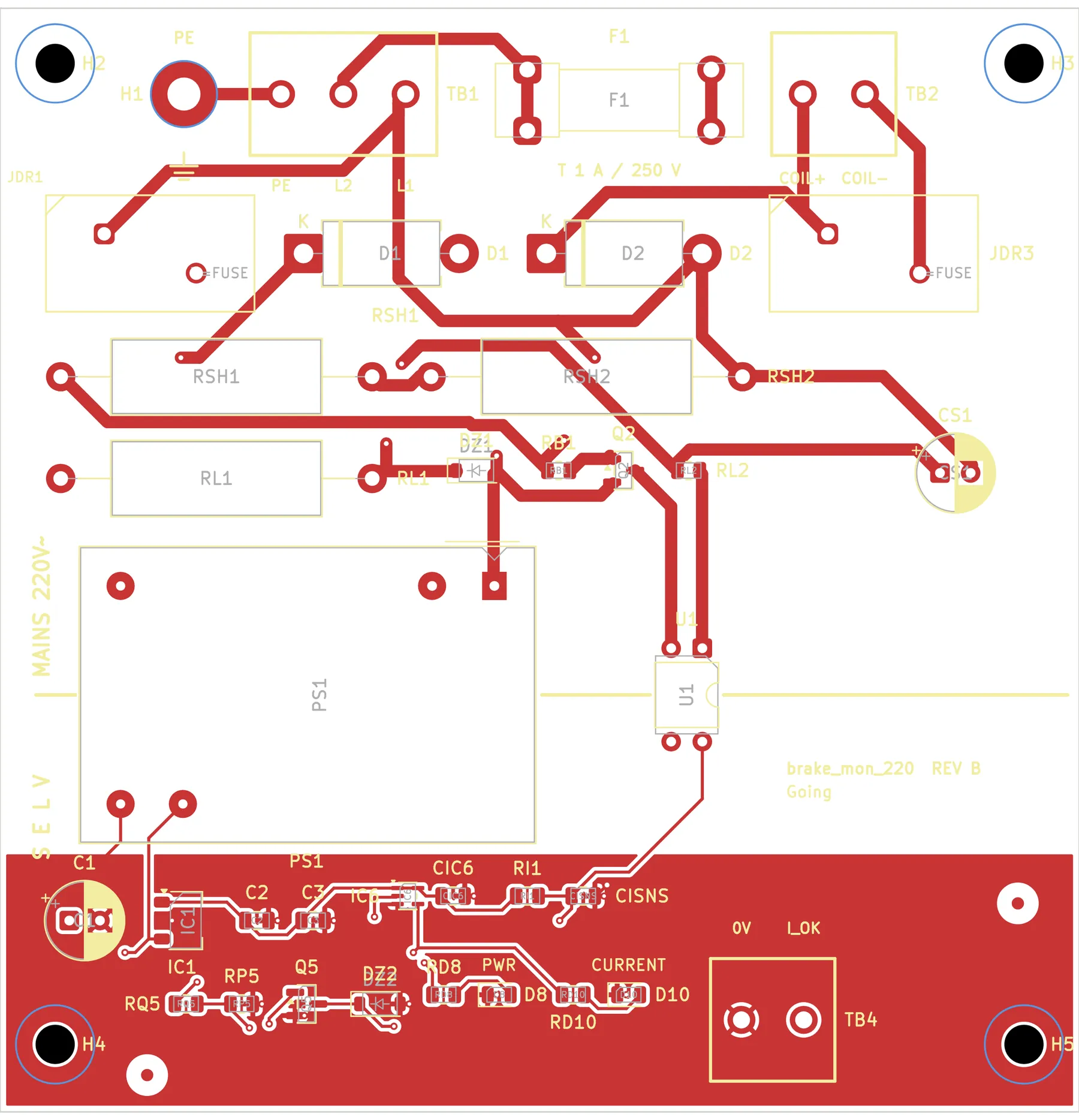
Part 11 went into measuring that line at length, so this post only covers what was left after the line had been respected everywhere.
Stale images went into the release three times
Packaging the outputs into a folder caught it three times.
| What | How it surfaced |
|---|---|
| Gerbers nine minutes older than the board | We fixed a 3D model and did not re-export |
| BOM and 2D artwork older than the source | Noticed by chance while packaging |
case_top.png showed the old enclosure (109 × 111) | Someone asked “didn’t you skip that image?” |
All three were caught, or missed, by eye. All three would have been caught by looking at one file timestamp. So we moved the rule into code.
Two different kinds of check were needed.
| What it asks | Scope | |
|---|---|---|
| Timestamp order | Is the output newer than its source | Cheap. Applied to everything |
| Regeneration diff | Did it actually come from that source | Expensive. Only where a regeneration path exists |
If the second passes, the first is redundant. But the first can be applied to every output, and the second only to things that can be rebuilt. That difference causes a problem further down.
The first run reported six failures. Five of the six were our own checker’s fault.
Following a false alarm led to a real one
“Gerber regeneration diff - 9 differ.” All nine layers reported as different. Opening one and comparing line by line, the difference was three lines.
%TF.CreationDate,2026-09-07T14:55:27+09:00*%   vs  ...T16:15:39+09:00*%
%TF.ProjectId,fab_snapshot,6661625f-...*%      vs  %TF.ProjectId,brake_mon_220,...*%
G04 Created by KiCad (PCBNEW 10.0.5) date ...  vs  ... 16:15:39*
The first and third are dates. Our normalisation had missed the
G04 ... Created by ... date line, so those were false alarms. The copper was identical.
The problem is the second line. %TF.ProjectId was fab_snapshot. The project name
in the Gerbers the fab receives was our temporary file name.
That file existed because kicad-cli refills the zones whenever it touches a board. This board has GND pours on both sides, so that refill becomes a way to ship a board nobody has measured. We were taking a snapshot and exporting from that instead. The decision was right, but we did not know the file name gets stamped into the output. The name was also being appended to the output file names, so a separate loop was running afterwards to rename them back.
The fix was one line: put the snapshot in a subfolder, under the board’s own name.
SNAPDIR=out/fab_snap
SNAP=$SNAPDIR/$N.kicad_pcb      # file name = board name
The renaming loop disappeared with it.
Not simply silencing the false alarm paid off this time. Following “why did it say that?” one step further turned up a real problem sitting right next to it.
The check was modifying what it checked
The second and third failures are more embarrassing.
The regeneration diff re-runs the generator. That generator writes to a fixed place under
out/. So the moment the diff runs, the working copy is overwritten and its timestamp
moves to now. Which means the timestamp check breaks because of the check. Three items
went red exactly that way, with nothing actually wrong.
We now hold the original bytes and timestamp and restore them once the diff is done.
The third one: we were reading timestamp order inside the release folder. cp stamps
the copy with the time of copying. So comparing output against source inside the
release gives you “the time we packaged it” for both, and the ordering information is
gone entirely. All six items reported -0 min.
Timestamp order is now read in the working folder, and whether the release matches the source is answered by the regeneration diff. That is exactly why the two checks were separated in the first place.
The enclosure render had no way to be regenerated
The real reason case_top.png was still the old enclosure turned up here.
The enclosure render had no generator. The WRL model for KiCad was built by an inline script each time, and the image was pulled by typing kicad-cli by hand. So when the geometry changed, the image quietly stayed old. And with no regeneration path, the only thing a checker could apply was a timestamp comparison.
The fix was to emit the STL and the WRL from the same box list. When the STL that goes to the slicer and the WRL that goes to the render come from the same geometry, neither can go stale on its own. A script now runs all the way through to the render in one line.
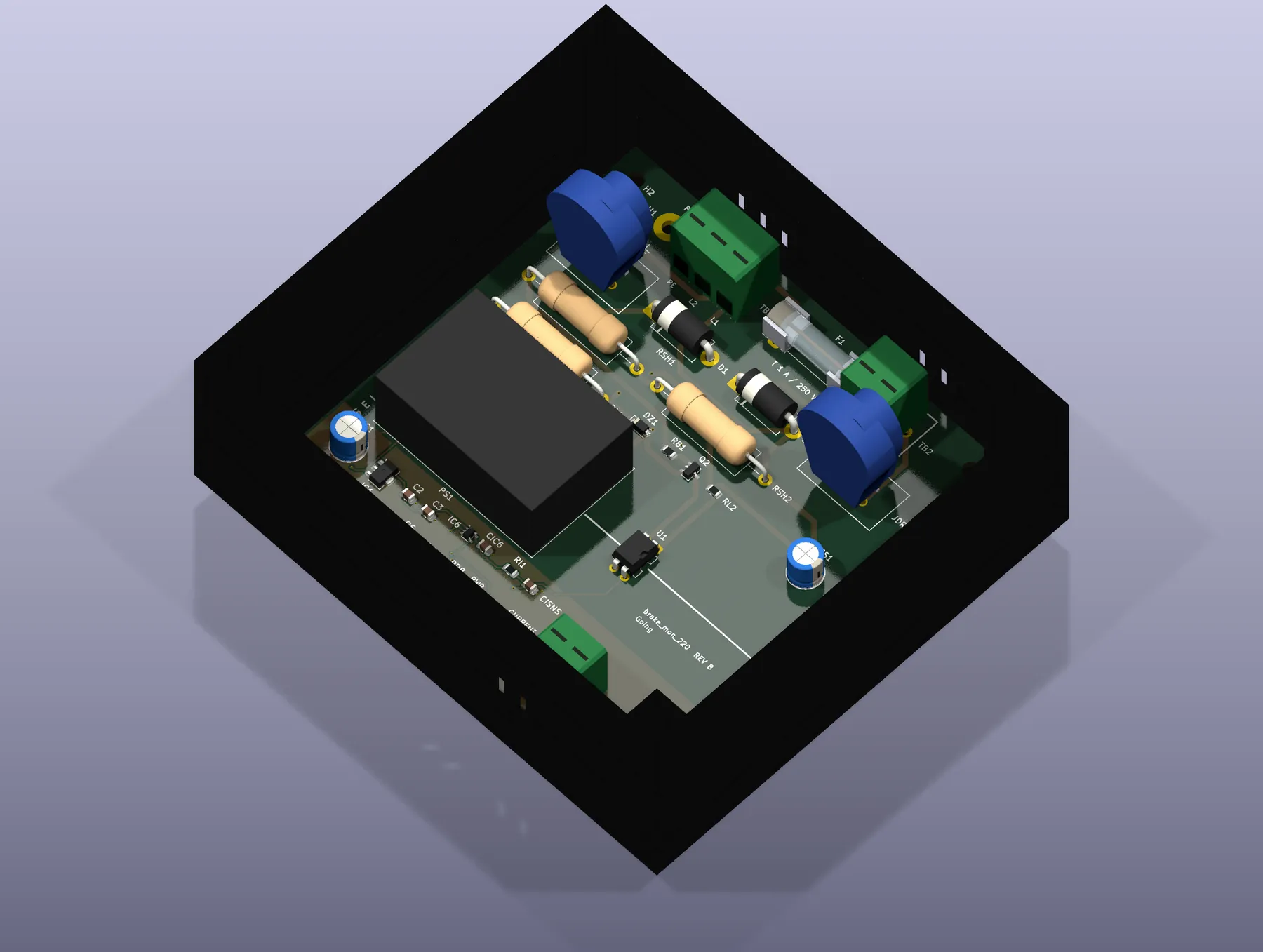
The enclosure is 109 × 97 × 40.3 mm. It is printed in-house, so the lid had to be designed too.
Three rounds of feedback came back while building it, and all three came from deciding on one dimension alone. The first version was nearly square, which left the terminal blocks 9.2 mm from the wall - you cannot plug a cable in like that. Lowering the Y axis into a rectangle brought the terminals against the top and bottom walls.
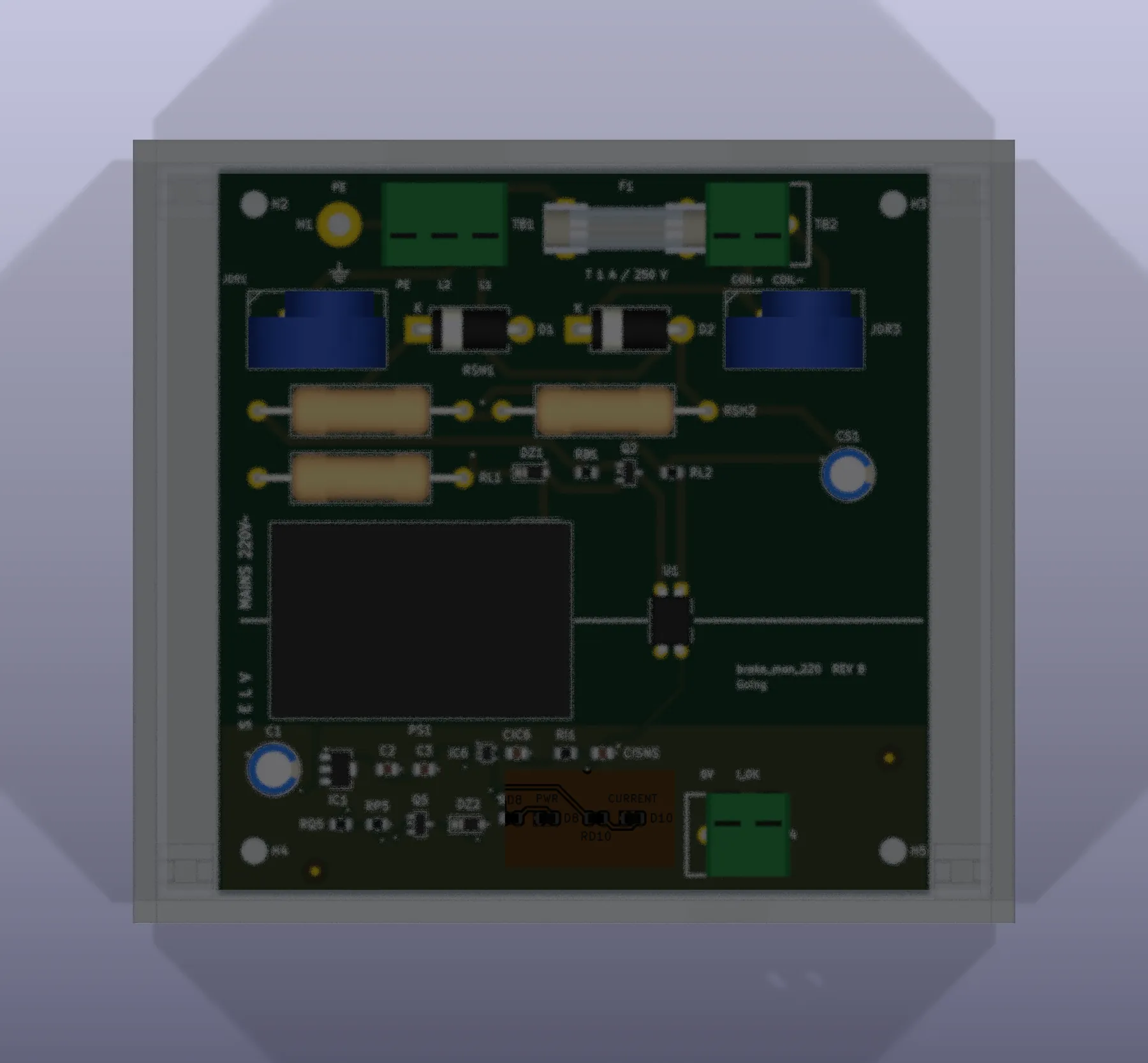
From above you can see one cable opening in each side wall per terminal pole. From the inner wall face to the terminal entry is 2.23 mm - the wall is the entry.

A section cut from the front. Below the board is 4 mm of standoff; above it is 30.2 mm of component space (tallest part 25.2 plus 5.0 clearance). The black block in the middle is the AC-DC converter.
Then we made the same mistake once more. Running the enclosure generator just to check a screw length rewrote the STL and WRL, pushed the timestamps, and broke verification again. Reading a report and writing files are now separate.
py case88.py --report # prints dimensions, writes nothingFilling in 21 MPNs - without inventing any
Verification ends here; real order preparation starts here.
This project had a policy: do not invent MPNs for generic passives. Stamping a vendor code onto an 0805 resistor or an X7R 25 V part means editing the BOM every time the supplier changes, and stamping one before the value is settled leaves a stale code behind. An MPN with no basis had in fact made it into this project’s BOM before.
But the actual point of that policy was “do not stamp an MPN you cannot justify,” not “leave MPNs empty.” And the order gate stayed red.
[FAIL] BOM: components with MPNs (13/34)With no distributor API credentials, we opened the manufacturers’ datasheets directly and read the ordering-code rules and dimensions. Twenty-one lines, not one of them written from memory.
Three of them are worth writing down.
The land chose the part
CS1 is a 10 µF / 50 V electrolytic. By value alone, UPW1H100MDD is correct. But that
part is 5 mm diameter on a 2.0 mm lead pitch. Our land is
CP_Radial_D6.3mm_P2.50mm - 2.5 mm pitch. It does not fit.
Within the same family, the 10 µF that steps up to 6.3 mm diameter on 2.5 mm pitch is the
100 V part. So we used UPW2A100MED. We did not raise the voltage; we matched the
case. CS1’s actual working voltage is the 15 V held by the zener beside it, so 50 or 100
is margin either way.
The part has to honour the Vf the design assumed
The two indicators had their resistors chosen on an assumed Vf of 2.0 V. D8 draws 3.0 mA through 3.3 kΩ at 12 V; D10 draws 2.0 mA through 1.5 kΩ on 5 V logic.
The common modern InGaN pure green has a Vf of 3.2 V. Fitting one drops D10 from 2.0 mA to 1.2 mA. So we picked from the AlGaInP family instead.
| MPN | Vf typ | Actual current | |
|---|---|---|---|
| D8 (PWR) | APT2012MGC | 2.1 V | (12 − 2.1)/3.3 k = 3.0 mA |
| D10 (CURRENT) | APT2012SURCK | 1.95 V | (5 − 1.95)/1.5 k = 2.0 mA |
Both land exactly on the numbers written in the design notes.
Similar names are the dangerous ones
The fuse spec was “ceramic HBC, breaking capacity 1500 A or better at 250 VAC,
IEC 60127-2 sheet 5.” The holder is a Schurter part, so we looked for a Schurter fuse, and
the first search hit, FST 5x20, was a glass tube with low breaking capacity. The
5 × 20 dimensions match, so it nearly went in as-is.
The right one is SPT 5x20. The datasheet says:
Time-Lag T, H = High Breaking Capacity (Ceramic Tube)
IEC 60127-2/5 · 250 VAC
Footnote 1) IEC: H = 1500 A @ 250 VAC, p.f. 0.7 - 0.8
1 A is 0001.2504. We cross-checked the digit positions against 1.6 A being 0001.2506
in the ordering table. This project has a precedent of a hand-typed MPN being off from the
value by a factor of ten.
If it has no land, it does not get counted
While filling in MPNs, this came out: the fuse was missing from the BOM.
The BOM is built by counting the footprints placed on the board. But the footprint at F1 is the clip holder. The fuse itself is a consumable that clips into it, so it has no land and never entered the count at all. The four enclosure lid screws were missing for the same reason.
Having no land does not mean you do not have to buy it. Without the fuse the board does not work, and without the lid screws the enclosure does not close.
Two more came out of the same pass.
D8 and D10 had collapsed into one line, because both had the value LED. Their MPNs
differ, so querying by value alone makes one of them disappear. Splitting green from red in
the table above is what that fix looks like.
Only 14 of 39 parts had an MPN field in the schematic. Fix the MPN table without regenerating the schematic and the BOM carries the new values while the schematic carries the old ones. Both are deliverables, so which part gets bought depends on who receives which file. We regenerated the schematic to bring it to 39/39.
Results - 34/34 MPNs and 17 release checks passing
The final numbers. Start and end, side by side:
| Metric | Start | End |
|---|---|---|
| Components with an MPN | 13 / 34 | 34 / 34 |
| BOM lines | 29 | 32, every line a confirmed MPN |
| Schematic MPN fields | 14 / 39 | 39 / 39 |
| Release verification | 6 items failing | 17 items all passing · 174 files, 22.5 MB |
| DRC | 0 violations · 0 unrouted | unchanged |
What stays with us - where the checks cannot see
In part 11 we wrote that the dangerous state is holding two rulers without knowing it. This time something slightly different came out.
The checks that let us say “it’s finished” each had a place they could not see.
- Count by footprint → parts without a land drop out silently
- Query by value → parts sharing a value but not an MPN collapse together
- Read timestamps inside the release folder →
cperases the ordering - An output with no regeneration path → there is no way to ask whether it is stale
None of the four is “the check was wrong.” All four are “there is somewhere the check does not look.” Which is why the result stayed green.
What we actually gained this time may not be the 21 MPNs but being able to ask the whole release the question again in one line. Every output now has a command that rebuilds it, and with that there is no need to scan for staleness by eye.
One more thing. The genuinely open item left on this board is that the terminal block rating is not in our internal records. It is an in-house part with no manufacturer MPN, and the library note says “confirm with the supplier.” We left it exactly as it is rather than inventing something.
The most important part of filling in MPNs is knowing which places must be left empty.
🔧 The earlier parts of this series cover why we started, the scale bug, the library, the routing failures, the measurement bug, the move to four layers, the last mile, the finished board, the review that followed it, the placement loop, and the isolation barrier of part 11.
Contact
- Email: [email protected]
- Instagram: https://www.instagram.com/going.sen/
- Website: https://intosen.com/kr/consult/
Comments
Enter a nickname to leave a comment, or sign in with Google or GitHub.