
Everything up to part 10 was a 24 V board. This one is a board with 220 V on it.
One thing to scope first. We have been drawing schematics and layouts for more than twenty years, but every one of those boards was low-voltage control. A motor brake rectifier is a first for us. Neither the rectifier circuit that drives an electromagnetic brake nor the isolation design of a board carrying mains voltage is a field we have worked in. So this board is not a product, it is a prototype we felt our way through with AI in a field we have never built in.
A motor brake is an electromagnet, so cutting the power lets a spring apply the brake. We wanted to build a board that feeds that electromagnet rectified DC and at the same time watches for the state where “the release command went out but current is still flowing.”
On the rectifier side there was almost nothing we could judge for ourselves. So we handed the judgement to the documents and the tools, and only checked whether those two agreed with each other. In the end this is not a story about a circuit. It is a story about that agreement check failing ten times.
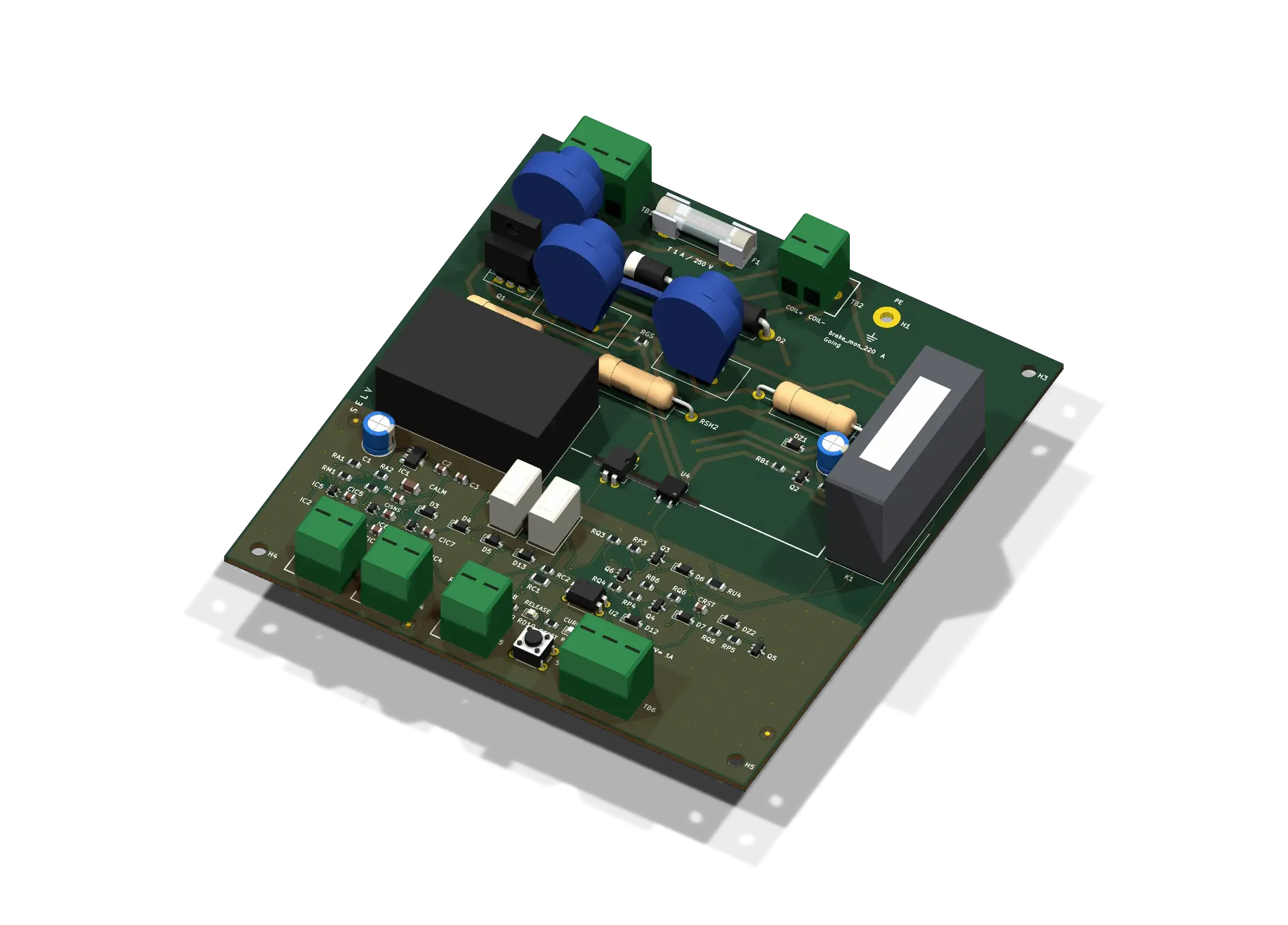
The finished board rendered in 3D. The mains area along the top carries three blue varistors
and a glass cartridge fuse, with the large relay on the right, while the low-voltage area at
the bottom is crowded with small parts and terminal blocks. The S E L V marking on the left
edge is the boundary this whole post is about.
The isolation barrier - creepage and clearance are set by different things
The isolation barrier is the line between the 220 V side and the low-voltage (SELV) side a person can touch, and it must not be crossed. Two different distances have to hold.
- Clearance - the shortest straight line through air
- Creepage - the distance along the surface of the board
They are decided by different things. Clearance is set by momentary overvoltage, creepage by the steady-state working voltage. We mixed the two at first and were feeding the 620 V surge figure into the creepage table. That inflates the requirement until no trace fits anywhere. For a while we kept concluding “this placement is impossible,” when what was impossible was not the placement but the requirement we had invented.
That much you can look up and correct. The next part was the problem.
Our grid disagreed with KiCad DRC ten times
Grid-based clearance judgement is the heart of this pipeline, because routing automatically means deciding for yourself whether a trace is allowed at a given spot. We lay down a 0.25 mm grid and paint each cell as blocked or free. That judgement differed from KiCad’s own DRC ten times. And all ten times ours was the more permissive one.
| # | Where it diverged | Symptom |
|---|---|---|
| 1 | Missing \1 in the DSN protect-marker substitution | Pre-existing routing was wiped out entirely and the router ran straight over it |
| 2 | Mistaking KiCad’s own (type route) for a protect marker | All 82 skipped, and “0 protected” passed as a green light |
| 3 | Lifetime of a temporary board object | The process died on random nets with no traceback |
| 4 | Net class clearance not applied | Laying 0.45 to 0.48 mm while DRC required 0.50 |
| 5 | A* budget exhaustion read as “no path” | A path existed, but it gave up at 120,000 pops |
| 6 | Pad radius taken as max(w,h)/2 | 158 rectangular pads underestimated |
| 7 | A package exception crossing the isolation barrier | A mains trace came within 3.88 mm of a SELV pad |
| 8 | A* not filtering the start and end layers | Reported routing “laid” that never touched the SMD pad |
| 9 | Component bodies not treated as obstacles | A pad ended up under a varistor, unsolderable |
| 10 | Candidate grid rounded to 1 mm | Reporting that an answer that existed did not |
Only number 7 is a different kind. The rest are cases where the routing fails or the tool dies. Number 7 is a defect that passes if you leave it alone.
A package exception cannot cross the isolation barrier - KiCad’s rule order
The package exception exists for a good reason. Under a dense IC you cannot apply the full clearance: if the pin pitch is 0.28 mm and the clearance demands 0.50 mm, no trace can attach to that pin at all. So inside a component body we allow an exception the size of that component’s pin pitch.
The problem was that this board has a component that straddles the barrier. On the safety relay one row of pins is 220 V and the opposite row is SELV. Our grid decided “this is inside the component, so the exception applies” and allowed a mains trace to come within 3.88 mm of that component’s SELV pad. The requirement for reinforced insulation is 5.00 mm.
KiCad caught it. The rule order is (pairwise → terminal block → package exception → barrier), and KiCad applies the last rule that matches. So the barrier beats the exception. Our grid was the only one that did not know the order.
soft = _need[n2] if crosses_barrier(net, n2) else _pkg_gap(ref)One line. And for as long as that line was missing, our gate stayed green.
What we took from this - the danger in automation is not that it produces a wrong answer, it is that it gives a wrong answer a green light. A gate passing does not mean the gate is right.
We fixed how we measured, not the tool - reach, why, unblock
Having nowhere to ask why something failed was the real problem. It took getting stuck in the same place about six times before we changed the approach. Until then it went: try to route, fail, blame the placement, try enlarging the board. Tens of minutes burned each round with nothing to show for it.
Nothing told us why it failed. A* only says “not found,” and there was no way to tell whether that meant no path existed or the budget had run out.
So we built three tools. All of them leave the board untouched and always terminate.
reach.py- answers “can you get from here to there” with a flood fill. It is O(cells), so it finishes in seconds, and when it cannot get through it prints the coordinates of the blocking wall and the name of the net that owns it.why.py- actually lays the routing, shows only the newly created violations with their coordinates, then puts the board back the way it was. Instead of “7 violations (threshold 5)” it tells you “2.29 mm from this pad on D1.”unblock.py- deletes nets one at a time in a snapshot only, counting how many have to come out before the path opens. No disk writes, no DRC, no rollback.
The effect was immediate. We asked reach.py about the net that would not close to the very
end, and it reported that it could only get to 1,040 of the board’s 470,000 cells. And the
wall was routing we had laid ourselves thirty minutes earlier. It was not the placement’s
fault.
unblock.py went one better and answered “pull these two out and it opens” in seconds. Before
that, getting the same answer meant removing, laying, relaying and running DRC every single
time. Each round took minutes, and when the walls came in a chain we had to pay that cost in
full before learning it was still blocked.
Body outline or pad - the moment we confirmed we were wrong
The location of the bottleneck was something we thought we had found. The channel between two varistors is 9.34 mm and two mains traces need 9.5 mm, so it misses by 0.16 mm and the parts have to move. It sounded plausible.
Measuring again, 9.34 was the body outline figure. Measured to the pads, which is what copper actually cares about, it was 17.55 mm. The channel was ample, and the bottleneck was not the placement but the routing order.
There is a law that keeps recurring in this project: measure the same board with two rulers and you get two answers, and the wrong one was always ours.
When routing cannot solve it, make a part - the insulated wire link
The last connection never went in. We got 171 of 172 connections, and one was left.
unblock.py told us exactly why. Three nets want the same channel and only two fit.
Changing the order only changed which net was left out (confirmed six times). Handing all
three to Freerouting gave the same result, and rotating the component put it in conflict with
34 pieces of surrounding routing.
On a two-layer board, the standard answer when the last trace will not go in is an insulated wire link. The wire passes over the board, so it drops out of the competition for copper channels entirely. It was not in the library, so we made one.
There was one more thing to learn here. To tell KiCad that “these two pads do not need to be joined in copper,” the net has to be split in two. Electrically it is the same node, but it is given two names, and a two-pin component (the wire) bridges them. The unrouted count then goes away.
And the new net has to inherit every isolation requirement the original net carried. Copying those across by hand means they quietly drop when a name changes, so we derived them from the table instead.
for (a, b), (v, why) in list(PAIR_V.items()):
    if a == "COIL_N":
        _hv("COIL_N_J", b, v, why + " (far side of the wire link)")
The position of the wire was not eyeballed either. We searched under three conditions - inside the area both ends can be reached by routing, satisfying the mains clearance, and both endpoints inside the mains area so the wire never crosses the barrier - which produced (21.00, 28.75) to (56.00, 26.50), a 35.1 mm wire.
Why parts vanished from the 3D render - model paths and offset
The 3D render check was the last thing we ran, and the relay, the fuse and the optocouplers were all missing.
The cause was deflating. The output path constant in the model generator still had the previous board’s name in it. We had copied the script without changing the path, so this project never got a 3D folder at all. Ten footprints were pointing at files that did not exist.
We built the five models that were missing. We did not substitute a similar standard model - doing that stands a different part up in the render, which is exactly the error the render was there to catch. Every dimension came from a datasheet or a footprint drawing, and the one value we could not find a source for (the fuse axis height) was left in a comment as “declared typical value (unverified)”.
We tripped here too. Swapping the model blocks in bulk, we overwrote every offset with 0,
and three varistors ended up outside their silkscreen boxes. The original was
(3.750, -1.600, 0). The rule depends on where the geometry was put: if the WRL geometry is
centred on the origin, the offset is (cx, -cy, 0); if it is in footprint coordinates,
it is 0. We should have read the original before overwriting it.
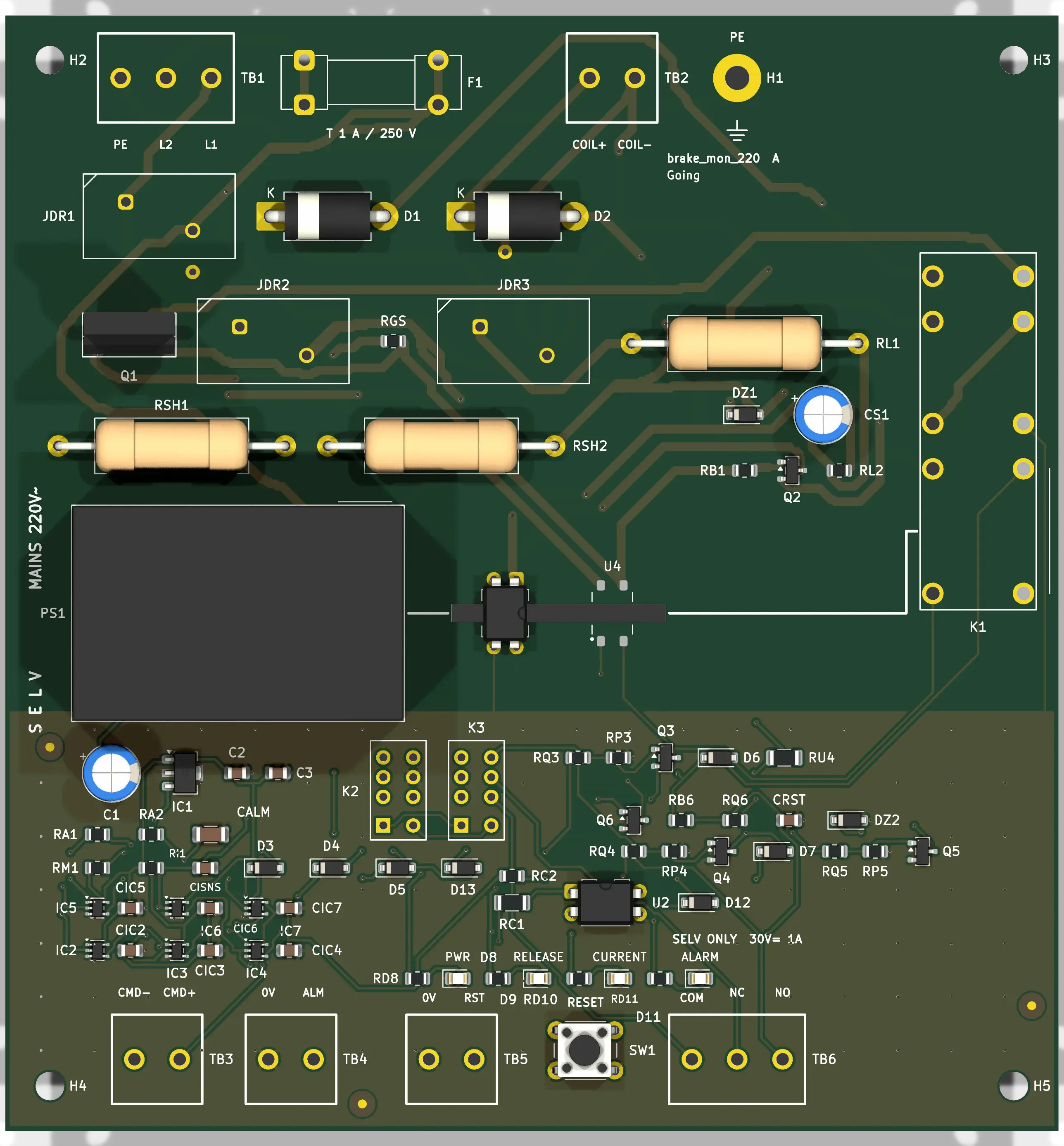
The top side once the routing was done. Between the MAINS 220V~ and S E L V markings on
the left edge, the board splits into an upper and a lower area, and an empty band runs between
them with nothing crossing it. That band is the isolation barrier, and all ten disagreements
in this post were about measuring it correctly.
Results - DRC 0, zero isolation violations
The final numbers. Start and end, side by side:
| Metric | Start | End |
|---|---|---|
| DRC violations | 163 | 0 |
| Unrouted component pads | 8 nets | 0 |
| Creepage and clearance | - | 26,702 pairs, 0 below spec |
| Isolation barrier | - | 0 violations |
118 × 125 mm, two layers, 96 parts, 1,185 track segments totalling 3,758 mm, 166 vias.
What stays with us - two rulers is the dangerous state
Of the ten disagreements, we found none on our own. Our tools were wrong ten times on this board, and all ten were caught either by KiCad or by changing the way we measured.
The most dangerous moment in building something with AI in a field you have never built in was not the moment of not knowing the answer. It was holding two different rulers without realising it. When our grid said “this is allowed here” and KiCad said “no,” we suspected KiCad more than once. All ten times we were the ones who were wrong.
So the real output this time may not be the board but the three tools. reach, why and
unblock - all three leave the board untouched, always terminate, and tell you why.
Having somewhere to ask before saying “it cannot be done” was the biggest difference.
The most dangerous moment in building something with AI in a field you have never built in is not not knowing the answer - it is holding two different rulers without realising it.
The earlier parts of this series cover why we started, the scale bug, the library, the routing failures, the measurement bug, the move to four layers, the last mile, the finished board, the review that followed it, and the placement loop.
Contact
- Email: [email protected]
- Instagram: https://www.instagram.com/going.sen/
- Website: https://intosen.com/kr/consult/
Comments
Enter a nickname to leave a comment, or sign in with Google or GitHub.