
Everything up to part 9 was about a single four-layer IO board. This time it is a new board - an RP2040 with DC24V input, four opto-isolated input channels, four relay output channels, four layers, 72×84 mm.
And this installment has one theme.
One-sentence summary
An unrouted net is not a conclusion. It is the starting point of the next investigation.
On this job we concluded three times that something was physically impossible. All three times we were wrong, and all three times the cause was not the board but our own code failing to see the channel.
1. Minimum manufacturing specs are not a variable you touch to make things fit
The via drill spec was the first thing we touched. A trace would not get through, so we shrank the via to 0.35/0.20 and the problem went away. DRC passed too. But that was not solving it, it was deferring it.
The feedback that came back was blunt.
“If you drill a via too small the via blows out, or the inner layer does not get drilled properly. Same with tracks - too thin and it will not print correctly unless it is a special PCB.”
So we fixed the spec by measurement. Opening the drill tables of nine in-house production CAM sets, the minimum drill was 0.300 to 0.305 mm without exception. The via stack in the original design said the same thing: standard via drill 0.305 / pad 0.610.
It cross-checked as well. On all nine boards these three counts match exactly.
board via count  =  drill tool 1 (0.30) count  =  0.61 pad aperture count
e.g.)  352 = 352 = 352,   173 = 173 = 173
The rule that came out of this:
A problem that goes away when you lower a manufacturing spec has usually been deferred rather than solved. Keep the spec as a fixed variable to the very end; what moves is the routing and the placement.
So we put a via gate at the end of the build. If a single via falls below spec, the build stops. A rule that lives only in a document is not followed - it has to be nailed into the code.
2. Next to a 0.4 mm pitch, a via genuinely does not belong
The QFN-56 pin pitch is 0.4 mm. We worked out on paper what a standard via would need there.
via radius 0.300 + clearance 0.150 + half-width of the neighbouring track 0.075 = 0.525 mm
required 0.525  >  available 0.400        → does not fit
This is not a tool defect, it is real geometry. What we got wrong here was the conclusion. We said the via does not fit so this pin cannot escape, when there was no reason to put a via there in the first place. Take the trace out of the pin in a parallel lane, run it to where the board opens up, and change layers there.
What was blocked was “a via next to the pin”, not “escaping that pin.” If you do not narrow down exactly what is impossible, you end up abandoning the possible along with it.

The area around the MCU once it was solved. The traces leaving the pins run out straight, in parallel lanes, and the vias are gathered where the lanes end and space opens up. The point of this picture is that there is not a single hole right beside a pin.
3. “Physically impossible” three times, all of them tool defects
| Our conclusion | The actual cause |
|---|---|
| “The lane ends are boxed in and cannot get out” | Pad size read with GetSizeX/Y (the pad’s own coordinate system), so width and height swap on rotated parts |
| “The maze cannot find a path” | A 0.10 grid adds one cell to the expansion, so 0.288 mm of available space was misjudged as needing 0.325 |
| “The pad is completely surrounded” | Treating the ground pour as a wall, so 1 mm of open space looked blocked |
All three times the screen said the same thing: the board is full.
We stepped on the GetSizeX/Y trap three times in this project alone.
So we turned the order into a rule.
- Measure in coordinates. Numbers, not impressions. Available space vs required width.
- If the available space exceeds the required width, suspect the tool.
- Unify the pass criteria. If the finishing loop and the final gate measure differently, the loop only improves against its own yardstick while the gate keeps seeing breaks.
- If it still remains, change the placement and run again.
4. Human-chosen placement breaks reproducibility - so we put it in the loop
The placement search loop (step 4 above) is the heart of this installment. Changing the placement really does change the result.
| What we changed | Unrouted |
|---|---|
| QFN halo 4.0 to 6.0 | 9 to 4 |
| QFN position (30,26) to (36,30) | 4 to 2 |
| Router once to best of 5 runs | Swinging between 1 and 9, stabilised at 1 |
We learned one more thing here. Router variance is larger than the placement effect. The same input yields anywhere from 1 to 20 incomplete routes. When variance dominates, do not fight to remove it - fold it into the automation and run several times, taking the best. It is not a lottery, it is a fixed cost (attempts × routing time).
So the final shape came out like this.
iterate over candidate placements, running the whole pipeline for each
  ├ route 5 times per candidate and keep the run with the fewest incomplete routes
  ├ stop and save immediately when unrouted 0 + shorts 0
  └ if no candidate reaches 0 → double the router attempts → grow the board (76×88 → 80×92 ...)
The point is that it does not stop when the candidates run out. Unless the parts genuinely fill the board, it escalates until something opens.
5. What actually ate the most time was the ways the loop itself dies
The automation infrastructure is where the time melted away once the placement loop started running - not in routing. All four failures were the silent kind.
1. Two builds used the same board file.
An earlier build was still running when we wiped the lock file with rm. The results mixed.
The answer to a lock is not to delete it but to separate the working directories.
2. The working copy did not keep its position in the tree.
The script finds the shared library through ROOT = two levels up, and copying only the board
folder made FootprintLoad return None, which killed placement outright.
3. A single sed line that made the copy had a syntax error.
The run script was never created at all, so all 12 candidates were tallied as failures. The
signal was that the log was 0 lines long, and we saw it late.
When candidates fail all in exactly the same way, suspect the loop rather than the candidates. Twelve out of twelve dying at the same point cannot be a design problem.
4. We killed a live build ourselves.
grep in the pipe was block-buffering, so a perfectly healthy build looked stalled in the
log. We decided it was dead and ran a global taskkill three times. Every candidate running
in parallel died with it, and we read that as the candidates failing to finish.
Alive or dead is judged by the process list, not by the log. To watch progress, use a
bash -x trace (stderr, unbuffered).
6. What the placement loop found
The answer the placement loop found was not the value we had believed to be optimal from our own measurements.
U1(36, 30), halo 5.0, board 72×84 → unrouted 0 / shorts 0The sweep made halo 6.0 look better, but the one that actually produced zero was 5.0. That is how large the router variance is, and it is why letting the loop run to the end beats a human picking from a sweep table.
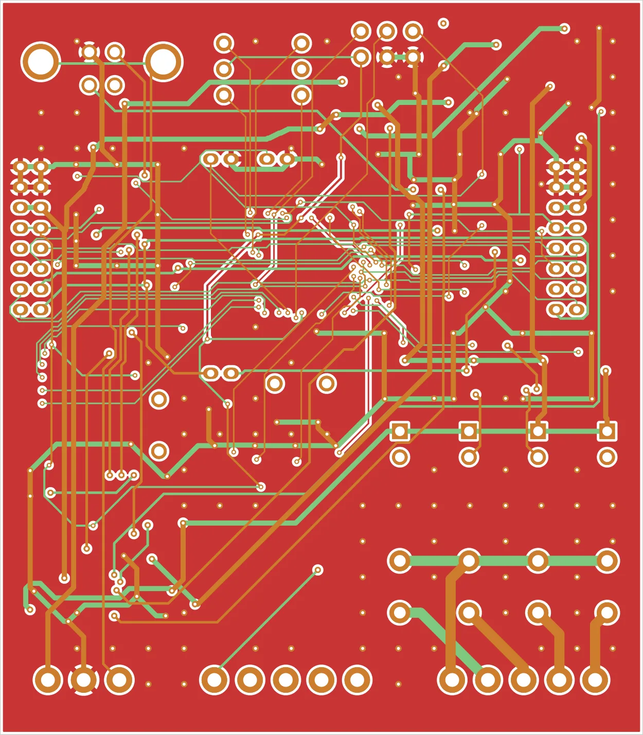
The result after rerouting with the placement the loop found. Orange is the top layer, green is inner-layer routing, and red is the inner-layer plane. The relay area at the bottom is sparse while the MCU area at the top is dense, which is exactly the character of this board - the blockage was always in the same place.
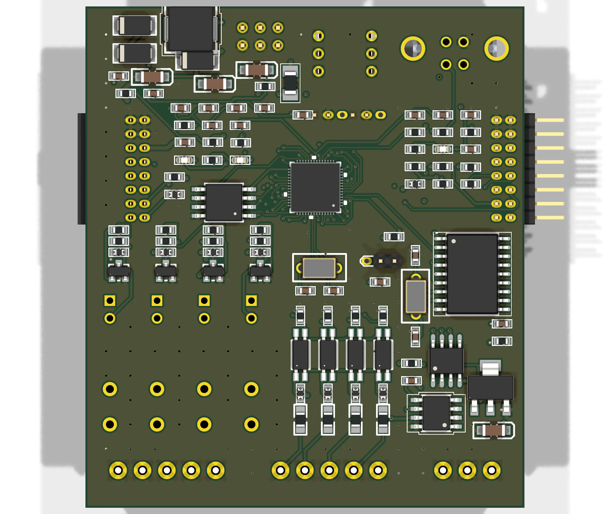
The bottom side of the same board. The square in the middle is the 0.4 mm pitch QFN, with resistors and capacitors packed tightly around it. This is what the dense area in the routing picture above actually looks like - with parts crowded together like this, the escape channels were bound to be that narrow.
For verification we did not trust the loop’s own numbers and measured again.
| Metric | Result |
|---|---|
| Netlist | NETS MATCH |
| DRC, 3 runs (worst value) | 0 unrouted, 0 shorts |
| Remaining violation | starved_thermal 1 (thermal relief - removing it would prevent soldering, so it stays) |
| 215 vias | all at or above 0.60/0.30 |
| Angles | 0 free angles |
The rules from this installment
Before closing a report that says it cannot be done, check that all four steps were taken: coordinates, tool, pass criteria, placement.
- Minimum manufacturing specs are a fixed variable to the very end. If lowering them makes the problem go away, it has been deferred
- Narrow down exactly what is impossible - “a via next to the pin” being blocked is not the same as “that pin escaping” being blocked
- When variance dominates, put the variance inside the automation (best-of-N)
- When every candidate fails identically, suspect the loop
- A log that looks stalled does not mean the process is dead - check the process
- Leaving the placement choice in human hands breaks reproducibility. It belongs inside the loop
An unrouted net is not a conclusion; it is a signal to work through coordinates, tool, pass criteria, and placement in that order.
The next installment will put this board side by side with nine in-house production drawings and take it apart - how the copper pours are laid, what can and cannot be read out of Gerbers, and a number we had written down incorrectly in the past that got corrected along the way.
Part 11 follows: the 220V isolation barrier. This time the board carries mains voltage, and the grid we use to measure the barrier disagreed with KiCad DRC ten times - every one of them in the more permissive direction.
The earlier parts of this series cover why we started, the scale bug, the library, the routing failures, the measurement bug, the move to four layers, the last mile, the finished board, and the review that followed it.
Contact
- Email: [email protected]
- Instagram: https://www.instagram.com/going.sen/
- Website: https://intosen.com/kr/consult/
Comments
Enter a nickname to leave a comment, or sign in with Google or GitHub.