
With the scale bug behind us, the next problem came into view. Until then we had been converting the PADS library ad hoc, pulling out only what each board needed. The same component ended up existing several times under different names, and conversion bugs had to be reproduced board by board.
So we tore it up. The PADS originals stay where they are, and we build a KiCad-native library from scratch.
- 1,214 footprints →
going.pretty - 857 symbols →
going.kicad_sym - Duplicates removed; values and ratings stored as fields so they drop straight into a BOM
One backslash broke the entire KiCad library
The KiCad symbol library we had just generated would not open: the entire library failed to load — not one broken symbol, all of them.
The cause was pin names. PADS wraps active-low signals in backslashes, like \RESET\.
Put that straight into a KiCad S-expression string and the backslash is read as an
escape character, which breaks the parenthesis balance of the whole file.
def esc(s):
    # Without escaping backslashes, KiCad cannot read the whole library
    return str(s).replace("\\", "\\\\").replace('"', '\\"')
We also moved the overbar notation to KiCad syntax: \RESET\ → ~{RESET}.
That is the price of generating files directly. One character invalidates an entire
file. So after building the library, we always open it once with kicad-cli.
The PADS pad definition had one field more
Footprint conversion came out wrong for 264 of the 1,214 footprints. All of them were parts with finger pads — the long rectangular kind.
A PADS pad definition looks like this.
OF (oval), 3 fields : <rotation> <length> <offset>
RF (rect), 4 fields : <corner radius> <rotation> <length> <offset>
RF carries an extra corner radius at the front. Reading the fields at the same
positions shifted rotation into length and length into offset, one slot over. The
documentation does not spell this out, so we dumped the value distribution across 5,000
lines and worked backwards from “what range of values shows up in this position.”
3D models — three wrong guesses
3D model alignment was off even with correct footprints: components sat in the wrong place in the render, and we assumed the cause was offset.
| Attempt | Hypothesis | Result |
|---|---|---|
| 1 | The reference is the pad center, so an offset is needed | Wrong |
| 2 | The sign of the offset is inverted | Wrong |
| 3 | The origin is the component outline | Wrong |
Only after three misses did we change method. We stopped guessing and compared renders. Rendering once with offset 0 and putting it next to the original showed that 0 had been correct all along.
The real cause was a 90° rotation, and we found it by matching pad layout patterns. Rendering a DIP16 part at 0°, 90°, 180°, and 270° and comparing against the original gave the answer immediately.
One lesson stuck.
Align 3D models by measuring pad patterns, not by reasoning about them. Solving in your head what you could just look at only costs time.
16-channel IO board placement — as if drawn against a ruler
Channel placement on a 16-channel IO board repeats the same circuit once per channel. A human draws one channel and copies it. The automation does exactly the same.
We take the relative placement of one channel block straight from the original and space the channels at a constant interval. The result:
- Channel pitch exactly uniform at 6.00mm
- 8 input channels and 8 output channels congruent with each other
- Zero components spilling outside their channel block
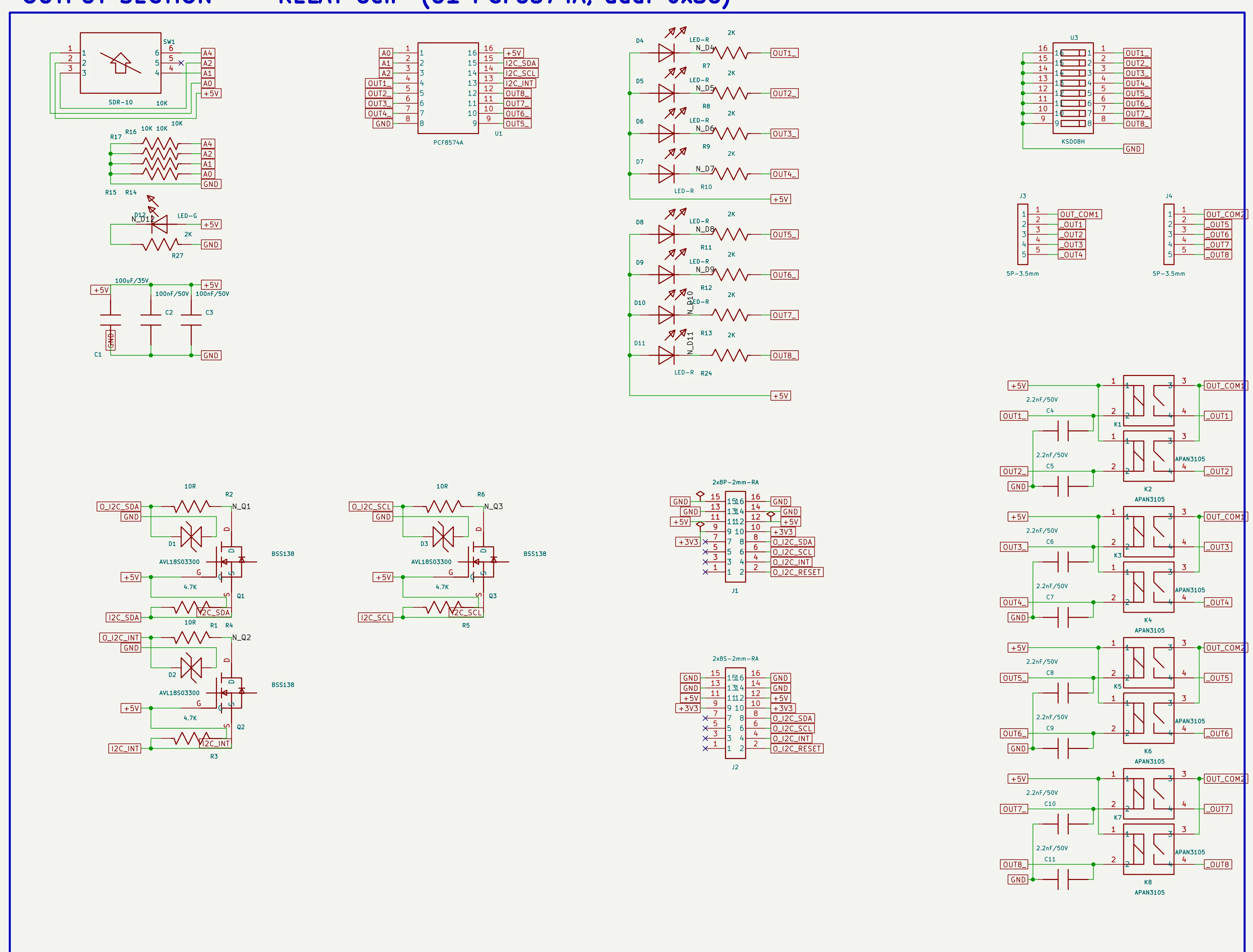
The converted symbols in actual use. The relays, optocouplers, resistors, and connectors all came across from our in-house library, and the pin numbers and names carry the values of the original decals. One shifted pin here changes the netlist silently.
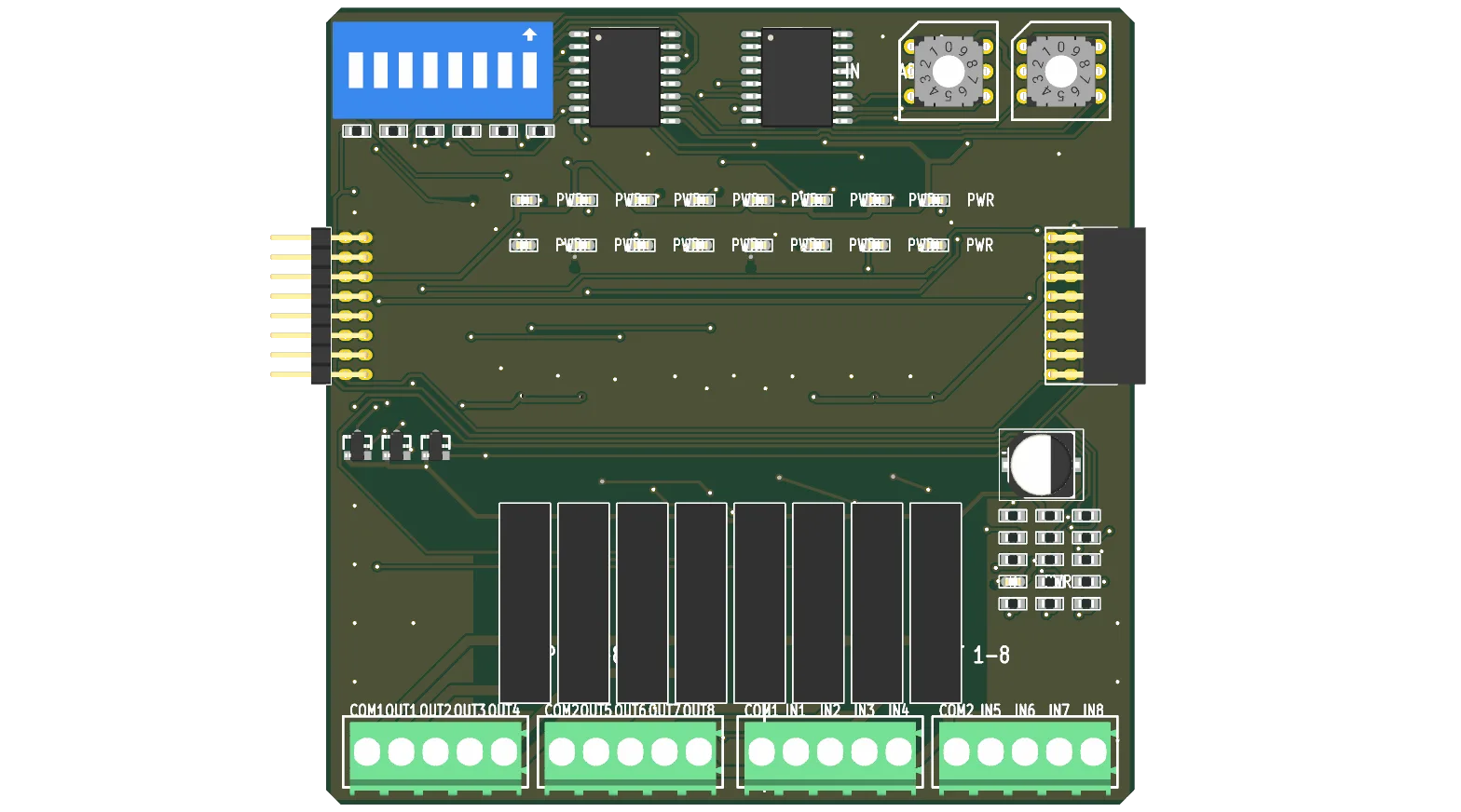
Uniform placement makes the next stage easier. Route one channel well and copy it to the rest — that was the theory, and it did not work nearly as well as expected. That story is Part 4.
Hard-coded dimension constants bite when the design changes
Hard-coded dimension constants burned us repeatedly at this stage. Values like the 28.35 terminal block body width, the 9.0 LED pitch, and the board expansion formula were written straight into the code, so every design change threw the whole placement off.
Now all of those come from exactly one place — the design intent file or the project settings. We would later get badly burned by defining trace width rules separately in each script, but that is Part 5.
Build the library once as a single set instead of converting it per board, and let every dimension constant come from exactly one place.
Next: routing. The 45° rule, staircases, traces ending in mid-air, traces squeezing between component pads. Plus the record of trying “just route the important nets by hand and hand the rest to the router” three different ways and making it worse all three times.
Part 4: The router will not cooperate — 45°, staircases, and three failures
Earlier in this series: Part 1, on deciding to automate, and Part 2, on the 1.5× board that passed every check.
Contact
- Email: [email protected]
- Instagram: https://www.instagram.com/going.sen/
- Website: https://intosen.com/kr/consult/
Comments
Enter a nickname to leave a comment, or sign in with Google or GitHub.