
With the pipeline working end to end, it was time to move to a real board. The target was an 8-channel relay output board we actually build and sell — 60 components.
The goal was not “close enough” but a 1
redesign: same parts, same connections, same size. That is the only way to find out whether the automation really works.Pulling the design intent out of the PADS original
PADS design files are where we had to extract everything we needed.
| Source | What we pull from it |
|---|---|
.asc (design ASCII) | Component coordinates, traces, board outline |
| LOGIC netlist | Which pin connects to which pin |
Library .d | Footprints (pad shape and position) |
| PL spreadsheet | Component values, ratings, part numbers |
We extracted the netlist from three places and cross-checked them. Trusting a single source lets a parser bug walk straight into the design. When all three agree, it is safe to believe.
PADS ASCII coordinate units — this is where it went wrong
PADS ASCII coordinates are integers, something like 43714500 85875000. Nowhere in
the file does it say what unit that is.
The file header says BASIC, and the magnitude of the values looked like nanometers.
So we read them as 1nm. The component pitches we computed from that looked plausible.
Everything looked plausible.
- All 60 component coordinates matched
- All 152 net pairs matched
- ERC 0, DRC 0
- Triple cross-check of the netlist passed
And the board was 1.5× too large.
Why the internal gates never caught the scale error
The internal gates we built all compare “a value we extracted” against “a value we generated.” If the parser reads everything 1.5× too large, then the coordinates are 1.5× too large, the board size is 1.5× too large, and the component spacing is 1.5× too large — and they all agree with each other beautifully. The ratios are preserved, so every internal check passes.
What caught it was a reference outside our files. The filename of the manufacturing CAM
data carried the board size: (51x81). Our result was 76×121.
51 × 1.5 = 76.5. 81 × 1.5 = 121.5. Exactly 1.5×.
The BASIC unit is 2/3 of a nanometer. In other words, divide by 1,500,000 to get
millimeters.
43714500 / 1,500,000 = 29.143 mm   ← correct
43714500 / 1,000,000 = 43.71  mm   ← what we had been doing
Checking against standard component pitches (2.54mm, 3.5mm, 1.27mm) would have caught this far sooner, but we were leaning on “all the internal checks passed, so it must be right.”
The worse part came next — dismissing external evidence
The first thing we said after seeing that number was this.
“That CAM is probably from a different revision.”
We dismissed external evidence as an exception, because we did not want to give up the assumption that our own number was correct. Fortunately the CAM for another board was off by the same ratio, so it collapsed quickly — but that one sentence nearly cost us hours.
So we nailed down one more rule.
When external evidence disagrees with our number, suspect our side first.
The library and placement we rebuilt after the scale fix
The coordinate scale fix made the board size match the original. But we had already carried the 1.5× error into the following stages, so the library and the placement had to be regenerated from scratch. The later you catch a mistake, the more you have to undo.
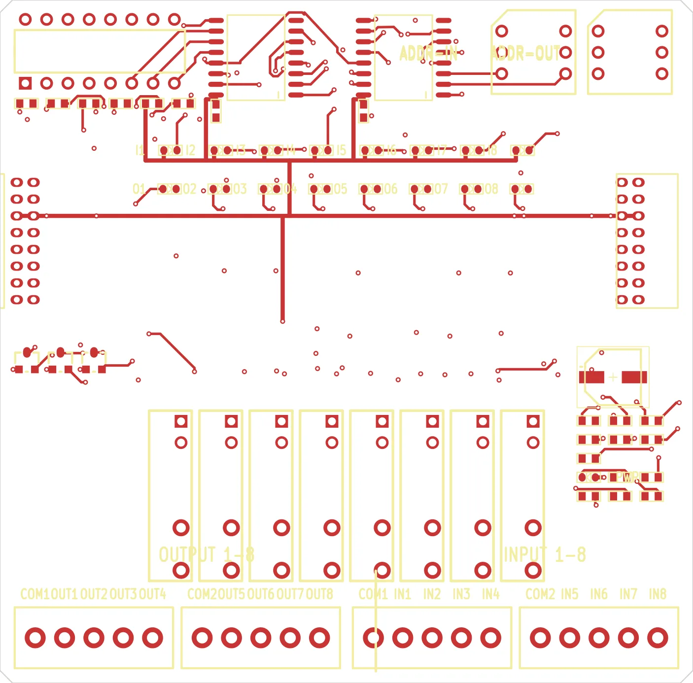
The top side after the scale fix. The outer border is the board outline, with the terminal blocks lined up along the bottom. When it was inflated 1.5×, this outline was a hand’s width bigger than the original and every internal gate still passed — because the components and the board were wrong by the same factor, together.
Since then, there is a first thing we always do when starting a new board.
- Read the actual board dimensions from the original manufacturing CAM
- Measure the pin pitch of a few components and check it against the standard values (1.27 / 2.54 / 3.5 / 5.08)
- Then run the pipeline
Every internal check can pass and the board can still be wrong, until you compare it against a measured dimension from outside your own files.
Next: the library. Rebuilding 1,214 PADS footprints and 857 symbols as native KiCad, where a single backslash made the entire library unreadable — plus three consecutive wrong guesses about 3D model placement.
Part 3: Rebuilding the library and placing 127 components
Earlier in this series: Part 1, on why we decided to automate PCB layout.
Contact
- Email: [email protected]
- Instagram: https://www.instagram.com/going.sen/
- Website: https://intosen.com/kr/consult/
Comments
Enter a nickname to leave a comment, or sign in with Google or GitHub.