
We already had a node that polls RS485 sensors and pushes the readings out over LoRa, but the three boards were lying loose on a desk. It needed an enclosure.
- Assembly: RAK19011 baseboard + RAK11310 LoRa core + TTL-to-RS485 converter board
- I/O: 5 V adapter (DC jack) · RS485 3-pole terminal · SMA external dipole antenna
- Result: 109 × 80 × 28 mm, two-piece screw assembly, 2 STL files
- Tools: Blender 5.1 + BlenderMCP + Claude Code
It is the same stack as our earlier write-up on building four 3D-printed cases, except this time we got a great deal more wrong. That is what this post is about.
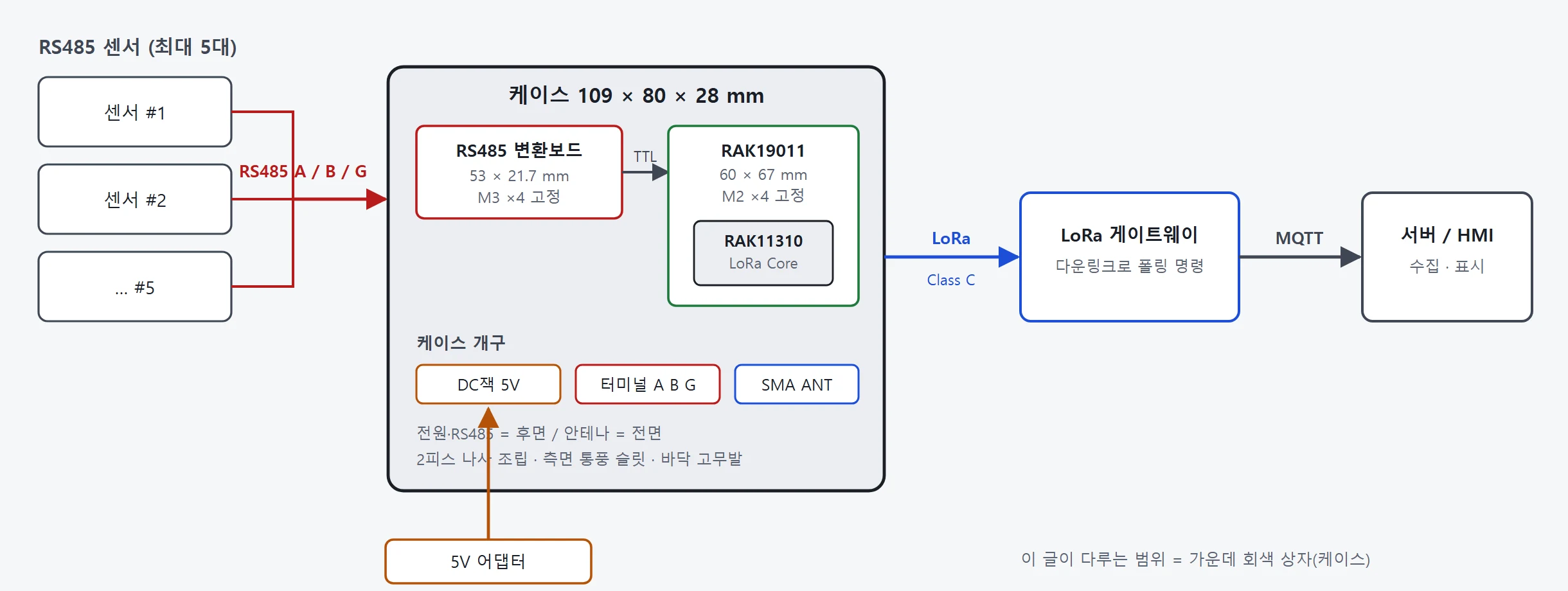
A node that queries sensors over RS485 and pushes the values up over LoRa. This post covers only the grey box in the middle — the enclosure holding the three boards.
What existed before the enclosure
The firmware and tools were already running. Getting the radio working came first, then impersonating a sensor with a PC-side simulator, then the polling loop and the monitor window — all covered in parts one through three of this series.
The enclosure exists because there was no box to put any of it in. Turning three loose boards on a desk into a product was what remained.
We misread the power module link at the very start
“I want to build a product using a LoRa module and a power module — the one linked on the site — on a RAK19011 board, and I need an enclosure for it.”
The AliExpress product link, read literally, was a power module. But AliExpress blocked the product page as a bot, so neither WebFetch nor a browser loaded anything beyond the footer.
There was a fork in the road here. Between the price point (₩2,580) and the context, we could have gone with “probably a small DC-DC buck converter” and moved on. That is exactly what we did, and we even reserved space for a buck converter inside the case.
A few exchanges later the truth came out.
“I’m using the RS485 converter board from that link to convert TTL levels to RS485 for the communication.”
Not a power module — an RS485 converter board. Power comes straight from a 5 V adapter, so no buck converter was needed at all. The entire internal layout had to be redone.
When you cannot open the source material, ask instead of guessing. Obvious advice, and it breaks down most reliably at the exact moment the context feels obvious.
Pulling coordinates out of a datasheet drawing
The RAK19011 board outline is not a rectangle. It is a stepped polygon with four asymmetrically placed mounting holes. And the dimensional drawing in the RAKwireless datasheet does not spell out all of the hole coordinates. It is an image with only some dimension lines attached.
We looked for a STEP file and there was none. So we extracted the coordinates from the drawing image itself.
The mounting holes are color-coded
The RAK drawing highlights the four mounting holes in light green. Finding cluster centers with a color filter is far more accurate than eyeballing them.
gray = (abs(r-g)<10) & (abs(g-b)<10) & (r>70) & (r<120)   # board gray
# four light-green ring clusters -> center pixel coordinates
Set the scale from a known dimension, then verify with a different one
We derived the X scale from the two values printed on the drawing (top-left hole X=13.50, top-right hole X=52.00).
S = (641.0 - 300.2) px / (52.00 - 13.50) mm = 8.8519 px/mmThen we used that scale to compute a different hole, and the bottom-left one came out at X=5.00 mm — exactly the value printed on the drawing. That is an independent confirmation that the scale is right.
The Y axis cost us a detour
X landed on the first try; Y did not. The bottom of the board is stepped, which made the choice of origin ambiguous. The bottom of the left section and the bottom of the right-hand protrusion differ by 5 mm.
In the end we fixed the origin by back-calculating the topmost and bottommost board pixels through the X scale.
| Hole | X (mm) | Y (mm) | Against the drawing |
|---|---|---|---|
| Top-left | 13.50 | 56.80 | drawing says 57.00 ✓ |
| Top-right | 52.00 | 64.12 | — |
| Bottom-left | 5.00 | 9.95 | left edge 5.00 + step 5.00 ✓ |
| Bottom-right | 52.00 | 2.70 | drawing says 2.70 ✓ |
Hole diameters came out the same way. Ø2.29–2.44 with Ø4.5 pads — M2.
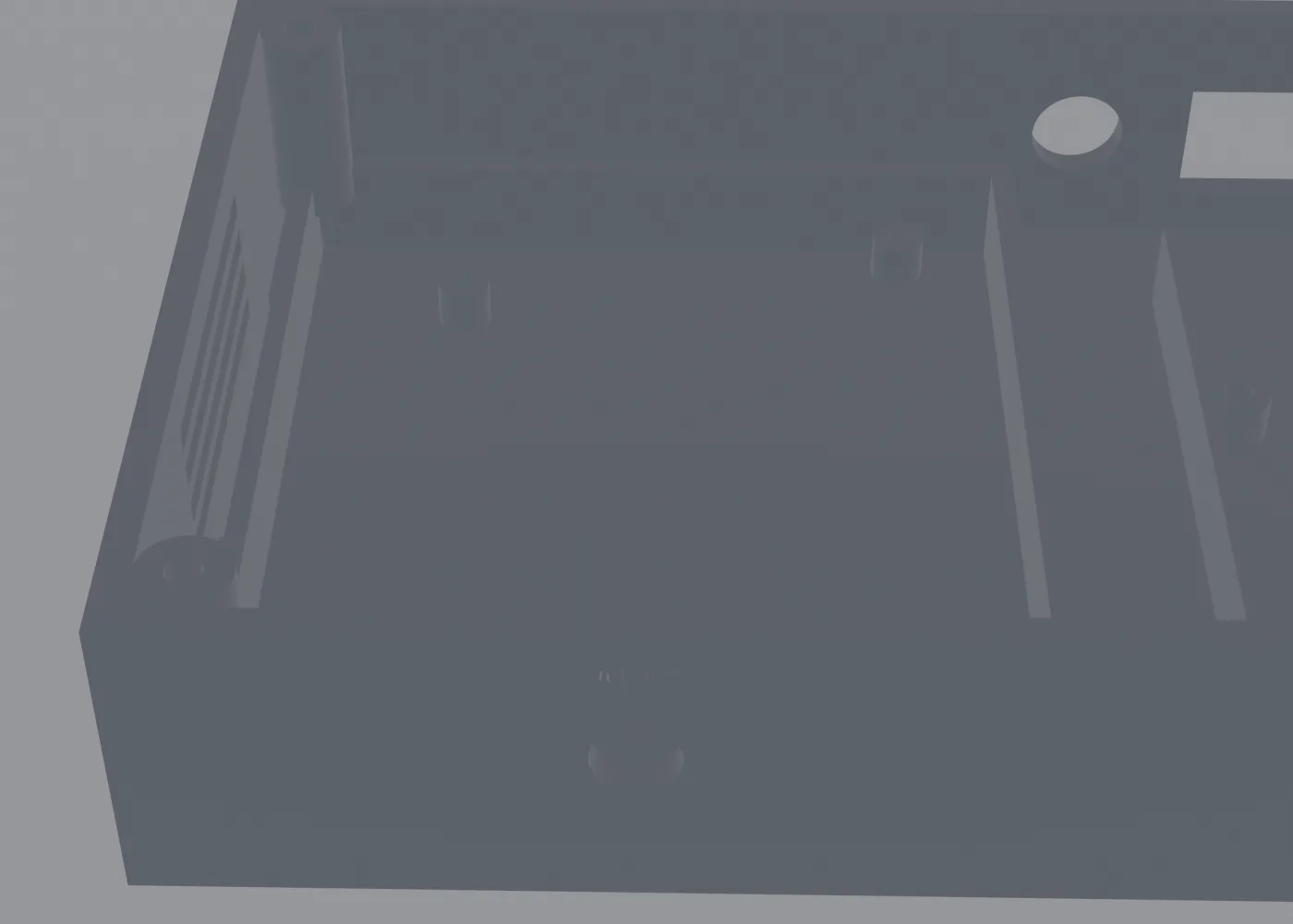
The boolean trap in Blender MCP
Applying a boolean in Blender MCP made the lid disappear entirely halfway through. More precisely, it had turned into a small cylinder (3.4 × 3.4 × 8.75).
The cause was bpy.ops.object.modifier_apply. In this environment, target and cutter end up swapped. We were trying to subtract screw holes from the lid, and what we got was the lid subtracted from the screw-hole cylinder. Only by printing dimensions at each step did we find where it broke.
1 plate   (99.0, 80.0, 2.5)
2 ring    (93.6, 74.6, 3.0)
3 joined  (99.0, 80.0, 5.5)      <- fine up to here
4 holes   (3.4, 3.4, 13.75)      <- breaks here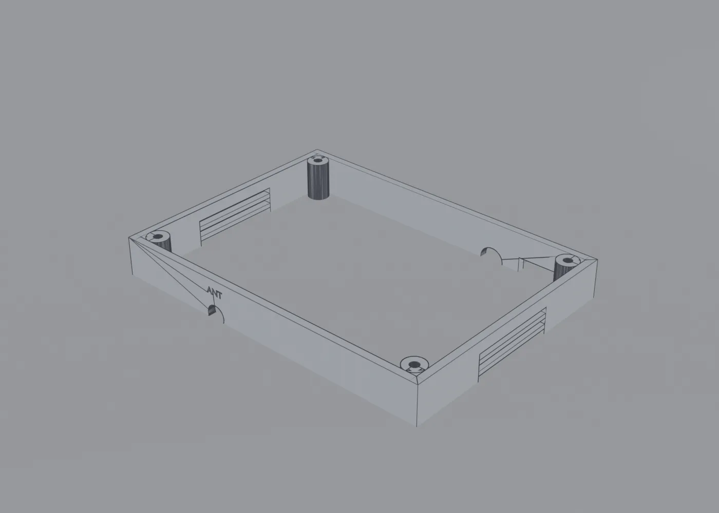
Dropping bpy.ops and baking the mesh directly through the depsgraph fixed it. It does not depend on context, so it is stable.
def bake(obj):
    """modifier_apply swaps target/cutter here, so bake through the depsgraph instead."""
    dg = bpy.context.evaluated_depsgraph_get()
    me = bpy.data.meshes.new_from_object(obj.evaluated_get(dg))
    obj.modifiers.clear()
    old = obj.data
    obj.data = me
    if old.users == 0:
        bpy.data.meshes.remove(old)

def bop(target, cutter, op):
    m = target.modifiers.new('B', 'BOOLEAN')
    m.object = cutter; m.operation = op; m.solver = 'EXACT'
    bake(target)
    bpy.data.objects.remove(cutter, do_unlink=True)
    return target
We added an assembly interference check before STL export
The assembly interference check runs automatically before exporting STLs. Duplicate two objects, apply an INTERSECT boolean, and measure the volume of the resulting mesh.
def inter(o1, o2, label):
    a = dup(o1, 'ca'); b = dup(o2, 'cb')
    m = a.modifiers.new('B', 'BOOLEAN')
    m.object = b; m.operation = 'INTERSECT'; m.solver = 'EXACT'
    bake(a)
    bm = bmesh.new(); bm.from_mesh(a.data)
    print('%-24s %9.4f  %s' % (label, bm.calc_volume(),
                               'OK' if len(bm.verts) == 0 else '*** OVERLAP ***'))
This part genuinely worked
The pre-STL check caught three assembly blockers.
- Lid lip ↔ corner screw boss — the lip corner (X 46.8–48.8) overlapped the boss (X 42–49), so the lid would not close at all. We cut a 7.6 × 7.6 notch into the lip corner.
- Vent slits ↔ lip — the topmost slit sat at the same height as the lip, so the lip was blocking the slit from the inside. We dropped the four slit rows by 3.5 mm each.
- Opening cutter eating into a boss — it should only cut the wall, but the cutter extended 20 mm in Y and punched a hole through an inner screw boss. We limited the cutter thickness to wall thickness + 2 mm.
Printed as they were, those three would have been wasted filament.
The interference check missed more assembly blockers than it caught
The assembly blockers the check missed are the real part. While the interference check kept reporting 0.0000 mm³ OK, three more assembly blockers turned up. All of them were caught by a person.
1. “How is the module even held? Are you just floating it in mid-air?”
We had explained that “the board sits in the rib pocket and the lid presses it down.” Except we never actually modeled anything that presses. The lid was a flat plate plus a lip, with 18 mm of empty space above the board. Nothing to press with.
The RS485 converter board was worse. The box in the render was a dummy marking out space, with no retention of any kind.
The description and the model had drifted apart, and the check cannot see that. Geometry that does not exist cannot interfere with anything.
2. “The terminal block is hitting the hole in the lid”
The check said BASE n RS485_term 0.0000 OK. A pass.
The actual clearance was 0.5 mm. Factor in 3D printing tolerance, the estimated terminal block height, and room for fingers during assembly, and 0.5 mm is interference. We passed it because the number was zero.
We raised the clearance to 4 mm.
| Item | Before | After |
|---|---|---|
| Terminal ↔ corner screw boss | 0.5 mm | 4.0 mm |
| Terminal ↔ lid lip | (not measured) | 5.4 mm |
| Wiring clearance | 7.5 mm | 11.0 mm |
3. The platform was pressing on solder joints
To support the RS485 board we laid a 3 mm platform on the floor — a plate supporting the entire underside of the board.
The check found nothing wrong, because we had modeled the dummy PCB as a flat plate. A real PCB has through-hole solder joints protruding from its underside. A flat support presses right on them.
We removed the platform and left only the four bosses. There is now 4 mm of clearance under the board.
4. A connector body passed straight through the board
We initially placed the DC jack and the RS485 terminal in the middle of the rear wall — that is, directly behind the main board. There was 4 mm of clearance behind the board.
A panel-mount DC jack intrudes about 20 mm inward. With a board 4 mm behind it, they collide. The reason the check missed it is simple: we never modeled the jack body. We only cut the hole.
We moved every connector to the right-hand bay, where there is no board, or above board height.
- DC jack · RS485 → right bay (no board)
- SMA → front face but at z=14 mm, passing above the top surface of the board
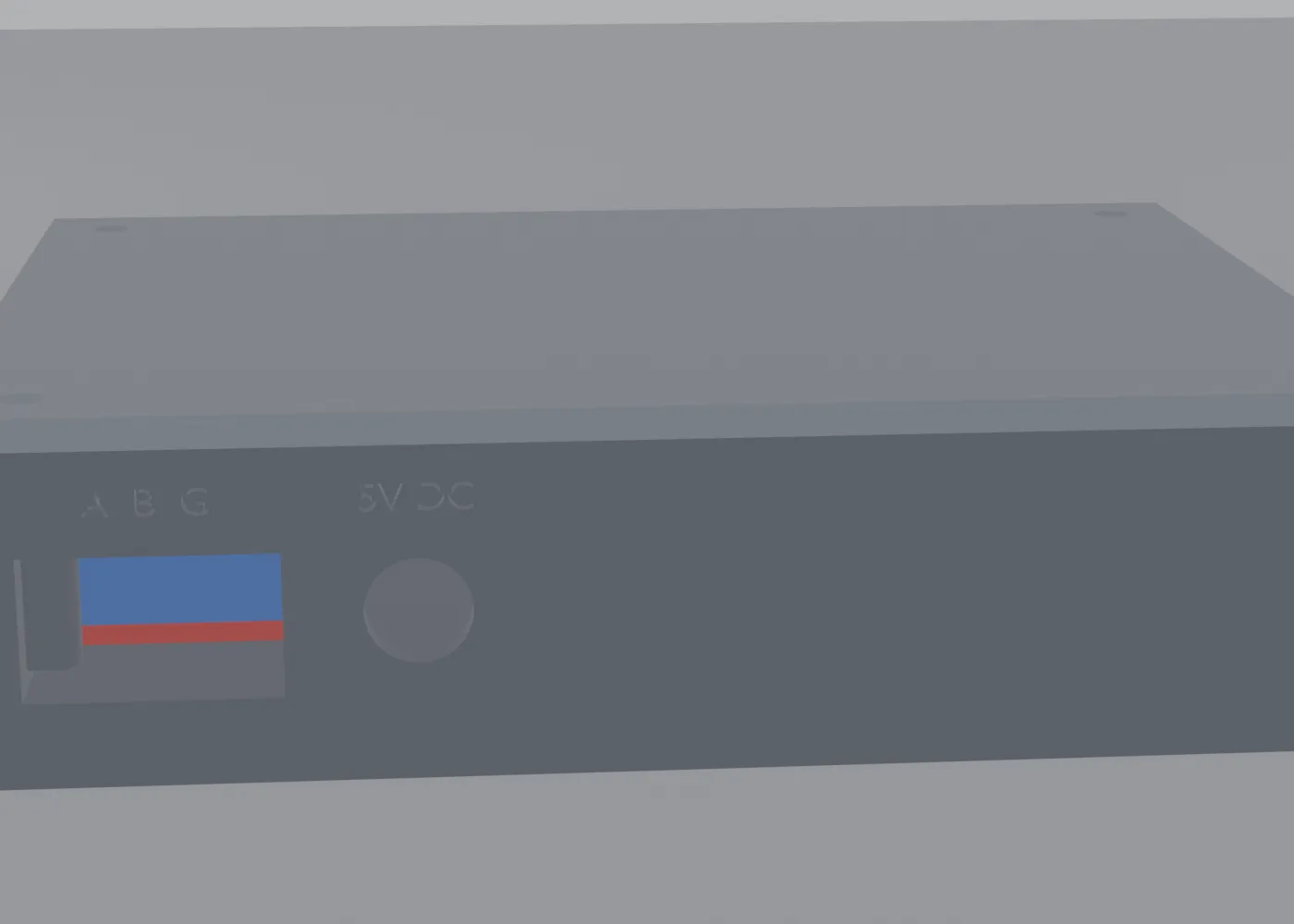
5. And then the bosses were simply not there
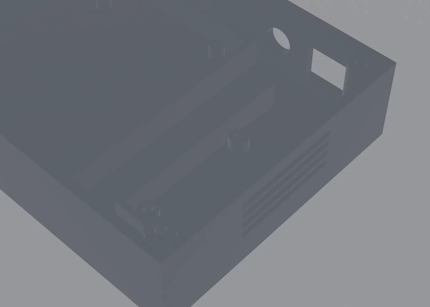
The one that hid the longest. We built the screw bosses and pocket ribs, looked at the render, decided it was fine, and moved on. In reality, every feature that touches the floor had vanished.
The cause is Blender’s EXACT solver and coplanar UNION. When the bottom face of a boss (z=2.5) exactly matches the top face of the case floor (z=2.5), the UNION silently fails. No error, just missing geometry.
An interference check can never catch this. Geometry that does not exist cannot interfere, so it kept reporting 0.0000 OK. The render did not give it away either — we mistook wall corners and vent-slit shadows for the ribs.
We only found it after building a separate check that asks whether the geometry is actually there. Place a small cylinder where a feature should be, intersect it with the case, and measure the volume.
def probe(x, y, z0, z1, r=1.5):
    """Check by volume whether anything exists at (x,y) between z0 and z1. 0 means nothing there."""
    a = dup(base)
    p = cylinder(r, z1 - z0, (x, y, (z0 + z1) / 2))
    intersect(a, p)
    return volume(a)
The results looked like this.
[RAK19011 mounting bosses]  vol=  0.00  *** MISSING ***  (all 4)
[RAK19011 pocket ribs]      vol=  0.00  *** MISSING ***  (all 4)
[RS485 mounting bosses]     vol=  0.00  *** MISSING ***  (all 4)
[RS485 pocket ribs]         vol=  0.00  *** MISSING ***  (all 3)
[Corner screw bosses]       vol= 12.19  OK
Only the corner screw bosses survived. They were the one feature that starts at z=8 and never touches the floor. That was the decisive hint.
The fix is one line. Make any feature that sits on the floor sink 0.5 mm into it, so the contact faces do not coincide and the UNION behaves.
MERGE = 0.5   # features unioned onto the floor must sink into it (avoids coplanar UNION)
base = bop(base, cyl('t', POST_D/2, STANDOFF + MERGE,
                     (x, y, FLOOR + STANDOFF/2 - MERGE/2)), 'UNION')
After the fix, all 19 features passed. Only then did the bosses and ribs appear in the render.
What the interference check cannot see, in common
All five assembly failures had the same shape.
An interference check only compares geometry that we modeled. What is not in the model is not in the check.
- Solder joints → the dummy PCB was a flat plate, so they were not in the model
- Jack body → we cut the hole and never modeled the body
- Assembly clearance → 0.5 mm is still mathematically 0 mm³
- Retention feature → described in words, never built as geometry
- Vanished bosses → nothing there, so nothing to interfere with
The last one is the nastiest. The first four are cases where the check saw too little, but this is a case where the check ran perfectly and produced the opposite conclusion. The more geometry disappears, the better the interference score gets. So we split the checks into three kinds.
| Check | Question | Pass condition |
|---|---|---|
| Interference | Do these overlap? | 0 mm³ |
| Existence | Is what should be there actually there? | Greater than 0 |
| Clearance | Are they far enough apart? | measured value in mm |
For clearance we stopped looking only at whether a volume is zero and started printing the actual distance in mm.
--- clearance measurements ---
terminal rear edge Y=26.50   /  corner boss front face Y=30.50   -> clearance 4.00 mm
terminal top face z=17.10    /  lid lip underside z=22.50        -> clearance 5.40 mm
DC jack body end X=25.50     /  RS485 platform start X=26.70     -> clearance 1.20 mm
Framed that way, the question stops being “is it zero?” and becomes “is it enough?”
The RS485 converter board coordinates came from a product image too
The RS485 converter board’s mounting hole positions came back as a product photo when we asked — a picture with 53 mm and 21.7 mm dimension lines drawn on it.
We used the same method as the RAK drawing: take the scale from the bounding box of the red PCB area, then label the bright circles inside the board to extract their centers.
red = (r>110) & (r-g>45) & (r-b>45)          # board area
bright = (r>225) & (g>225) & (b>225) & inside # holes inside it
lab, n = ndimage.label(bright)
# accept only blobs of 250px or more whose width and height differ by 6px or less (circular)
The cross-check came out well. The ratio of the X scale to the Y scale was 1.013, meaning the drawing has no distortion.
| Hole | X (mm) | Y (mm) | Diameter (mm) |
|---|---|---|---|
| Bottom-left | 4.11 | 2.88 | 3.69 |
| Top-left | 4.08 | 18.84 | 3.63 |
| Bottom-right | 36.05 | 2.98 | 3.37 |
| Top-right | 35.97 | 18.80 | 3.46 |
The Y center is 10.86 and the board height is 21.7, so exactly half — the symmetry checks out. Diameters of 3.4–3.7 mean M3.
This was faster and more accurate than measuring with a ruler. An image with even one dimension line on it is enough to extract coordinates.
Final LoRa node enclosure specification
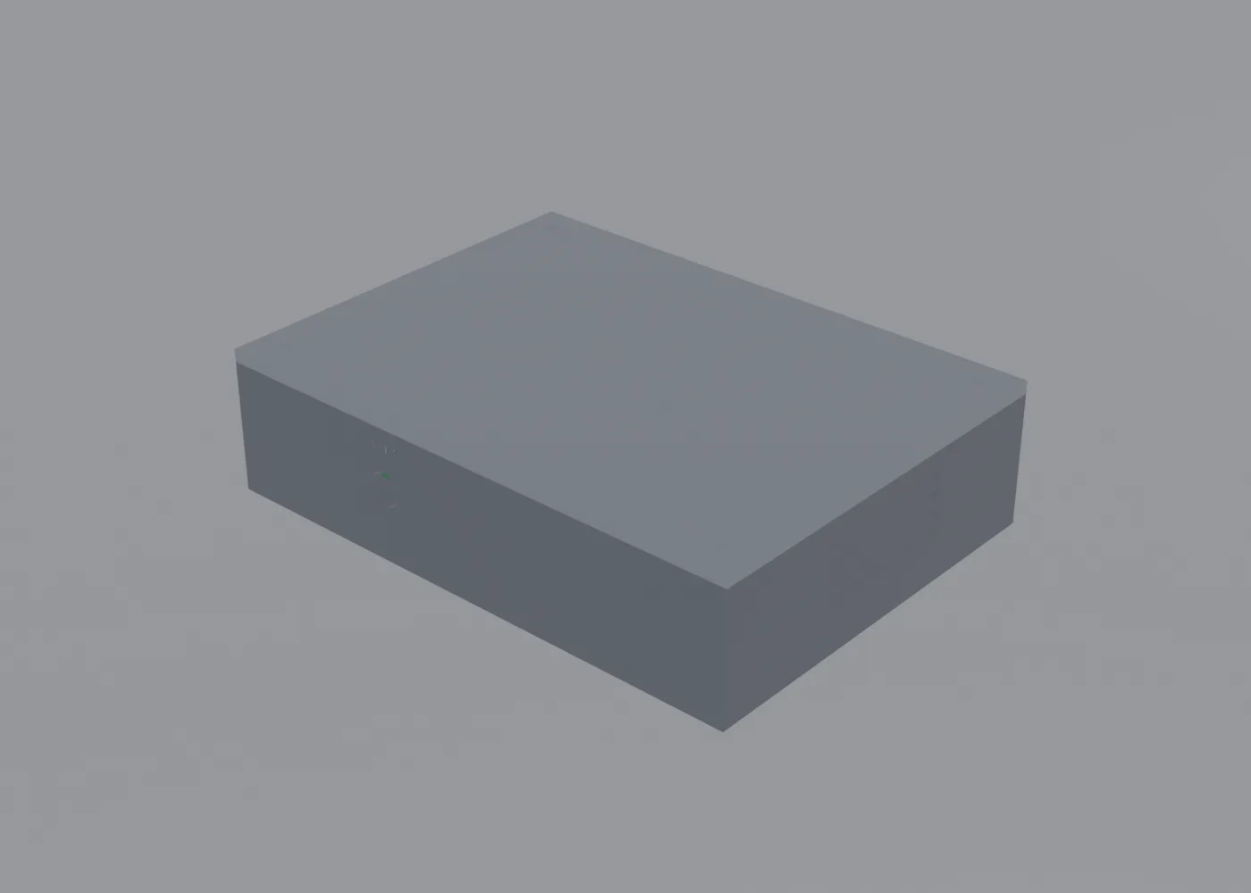
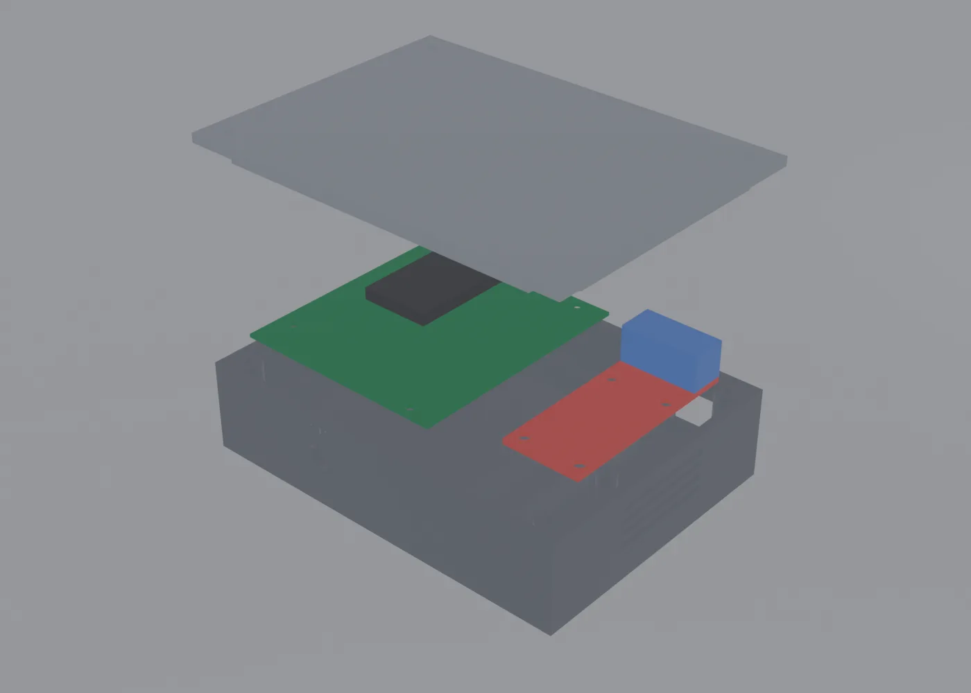
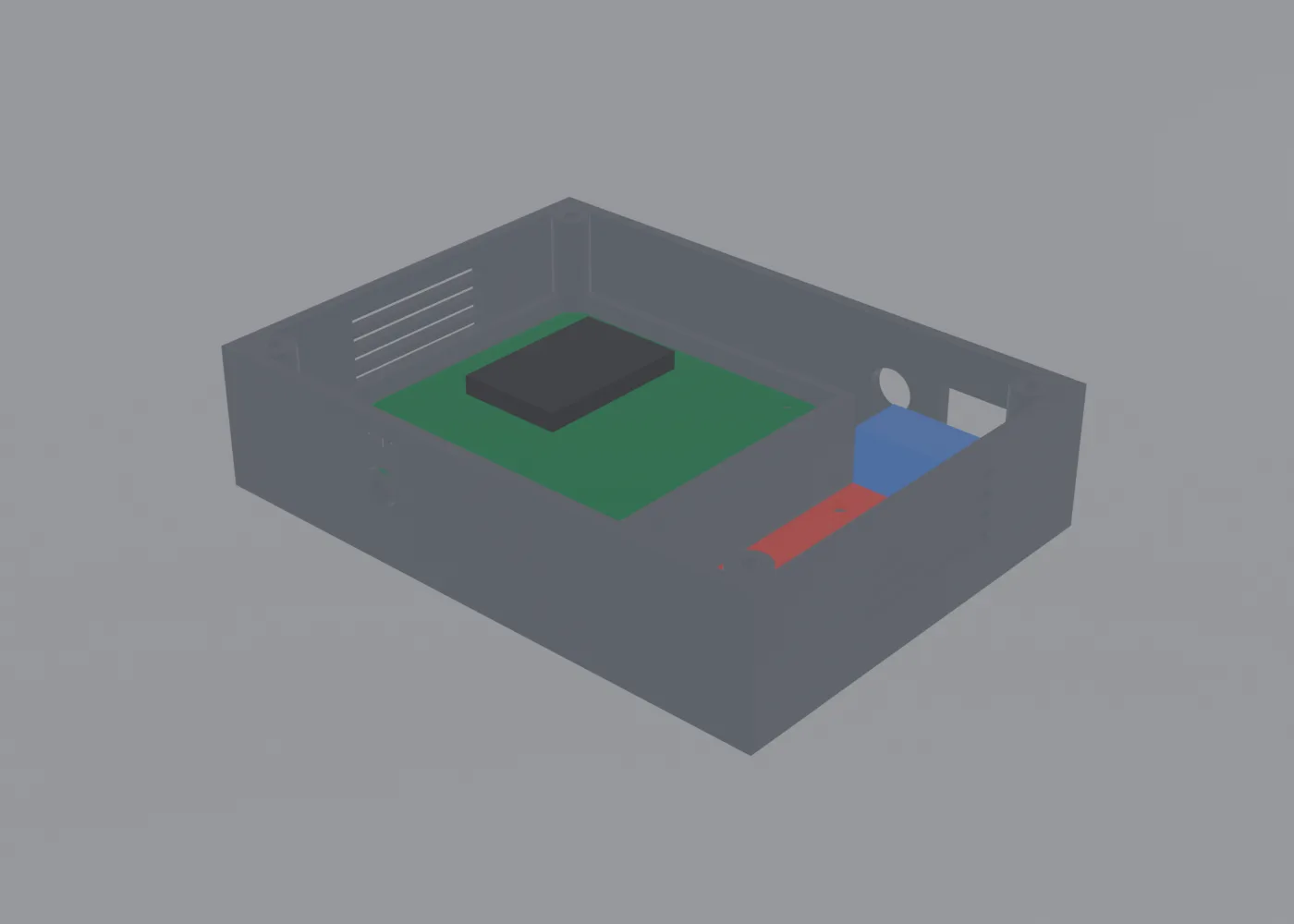
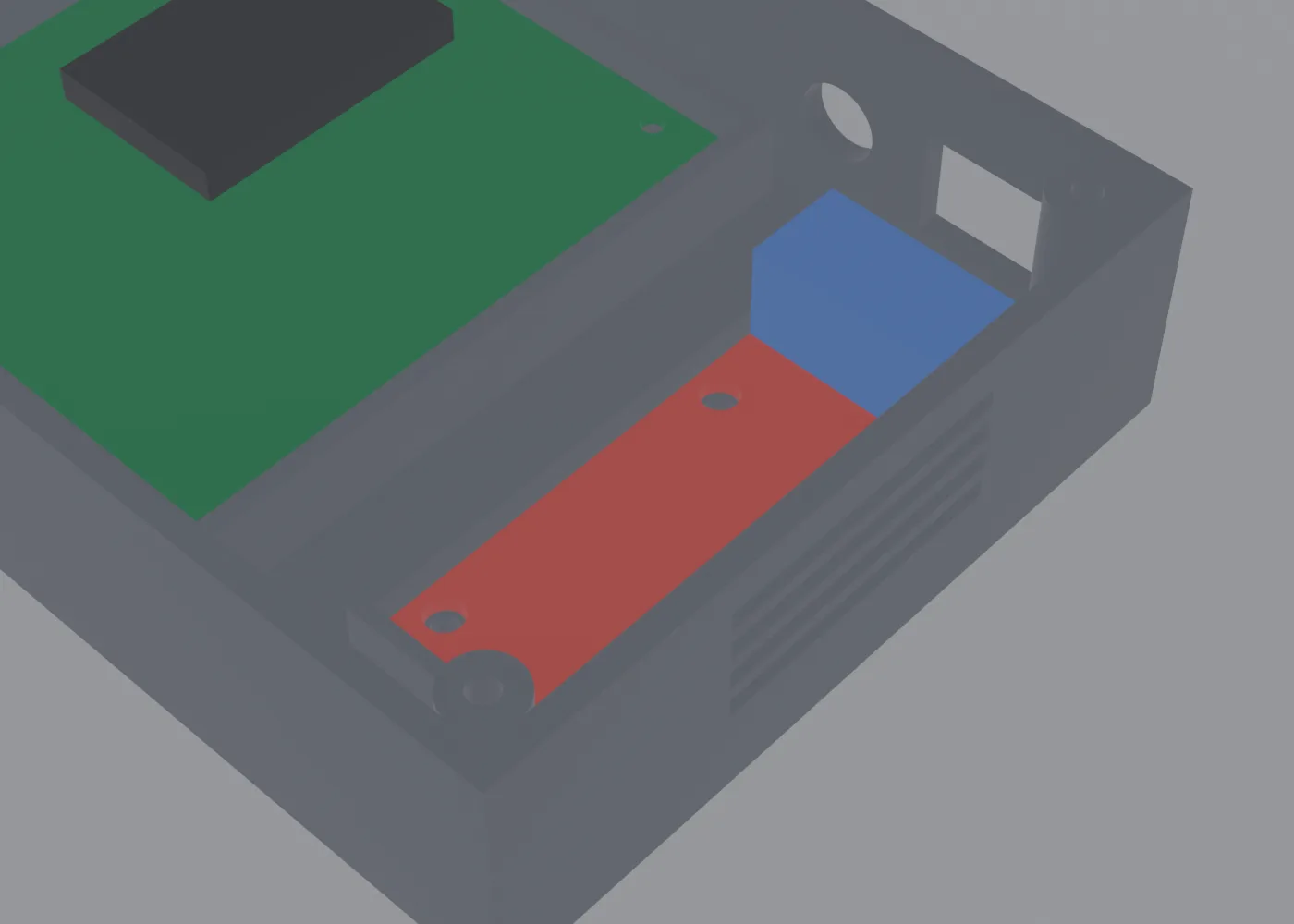
| Item | Value |
|---|---|
| Outer | 109 × 80 × 28 mm |
| Inner | 104 × 75 × 23 mm, 2.5 mm walls |
| Structure | Two-piece (body + lid), 3 mm lip fit |
| RAK19011 retention | M2 × 6 mm ×4 — boss Ø4.5, self-tap Ø1.7 |
| RS485 retention | M3 × 6–8 mm ×4 — boss Ø5.5, self-tap Ø2.5 (5.5 mm engagement) |
| Lid | M3 × 12–16 mm ×4 |
| Rear | DC jack Ø8 + RS485 3-pole opening, 5V DC / A B G engraved |
| Front | SMA Ø6.5, ANT engraved |
| Other | 4 rows of side vent slits on both sides, 10 × 10 rubber foot pads on the base |
Both STLs are non-manifold 0 and aligned to z=0 at the base. The lid is exported flipped so the flat plate meets the bed and the lip faces up, which means no supports.
The script is parametric, so changing the parameters at the top regenerates everything. Values we have not confirmed yet — the 18 mm component height above the board is an estimate — carry an unconfirmed comment in the source.
Details
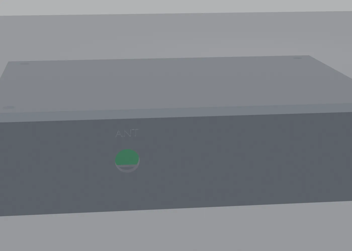
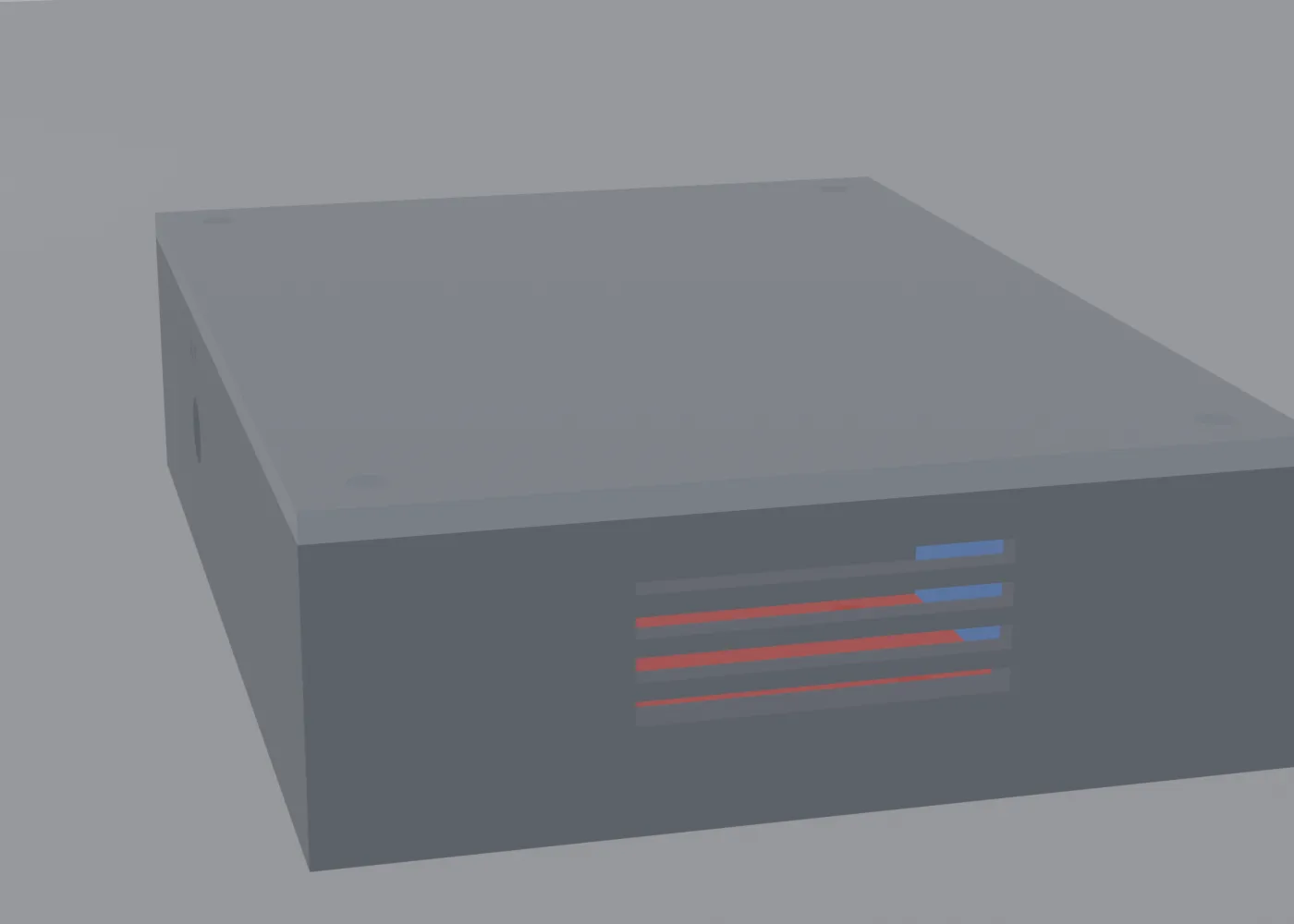
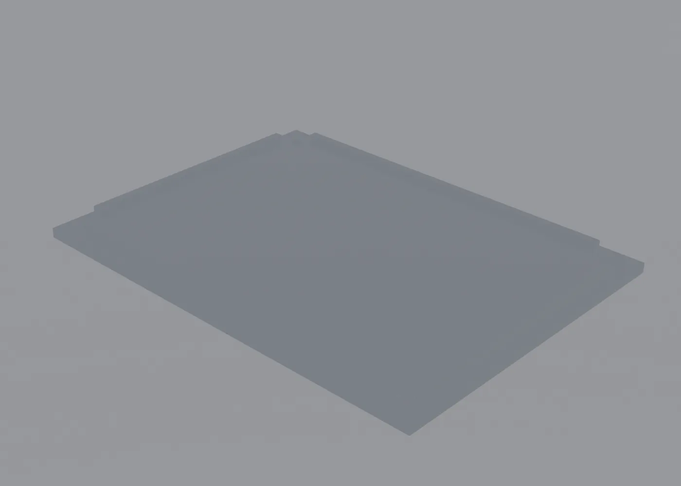
You can see the square cut taken out of the lid lip corner. That is where it collided with the corner screw boss and kept the lid from closing.
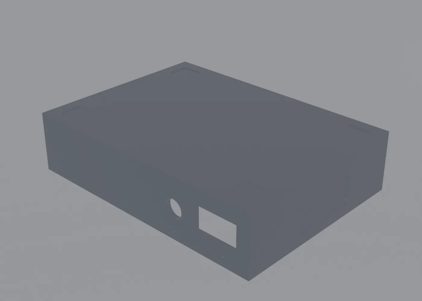
What we learned — zero interference is not assemblable
1. “Zero interference” and “the geometry exists” are completely different questions. When geometry disappears, the interference score improves. Without a separate check asking whether what you built is actually there, you will never find out that it is gone.
2. Zero interference is not the same as assemblable. Set clearances in mm and judge against that. Looking only at whether a volume is zero waves a 0.5 mm trap straight through.
3. The simplicity of a dummy model becomes the blind spot of the check. A flat PCB dummy knows nothing about solder joints, and a wall with only a hole in it knows nothing about the jack body. To trust a check result, you first have to know how much of the real object your model captures.
4. The description and the model can diverge. We wrote “the lid presses it down” and never built anything that presses. A function described in words has to be confirmed as geometry in the model.
5. A render is not evidence. We mistook wall corners and slit shadows for ribs and moved on satisfied. Trust the measured number over what you saw — but only when that number is answering the right question.
6. Ask about material you cannot open. We papered over one link with context and ended up redoing the entire internal layout.
7. A drawing image gives up its coordinates with a single dimension line. But always cross-check. Does a value derived from the X scale match another dimension on the drawing? Is the X/Y scale ratio close to 1? Only then can you trust the coordinates.
Without those five rounds of “you realize that won’t go together,” we would be printing a couple of enclosures that do not fit and hunting for the reason right about now.
Automated checks are fast. And yet the defect that hid the longest this time was not something the check failed to see, but something it passed while working perfectly. It kept answering “0 mm³, no problems” about a case whose bosses had disappeared entirely. A check only answers the question you asked it. It does not tell you what you are not asking.
Zero interference does not mean assemblable — it means nothing collides among the shapes that made it into the model.
▶️ Next in this series — the server says OK and half the data vanishes: We gathered nodes in these enclosures with Class C polling and pushed them to a server, and data sent every five minutes accumulated at ten-minute intervals. The story of three wrong guesses.
🔧 The whole series: part 1, silence and the sync word · part 2, the sensor simulator · part 3, the poller that does not wait · part 4 (this post) · part 5, debugging the uplink
Contact
- Email: [email protected]
- Instagram: https://www.instagram.com/going.sen/
- Website: https://intosen.com/kr/consult/
Comments
Enter a nickname to leave a comment, or sign in with Google or GitHub.