
There are three module types beside the main board. All are 51.0 × 81.5 mm, four layers, and connect over the 16-pin bus from part 1.
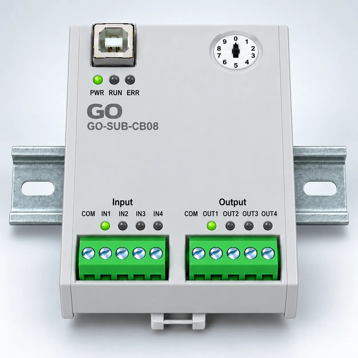
The CB08 front face with the cover on: the COM IN1~IN4 input terminals, the
COM OUT1~OUT4 output terminals, the USB port and the address switch.
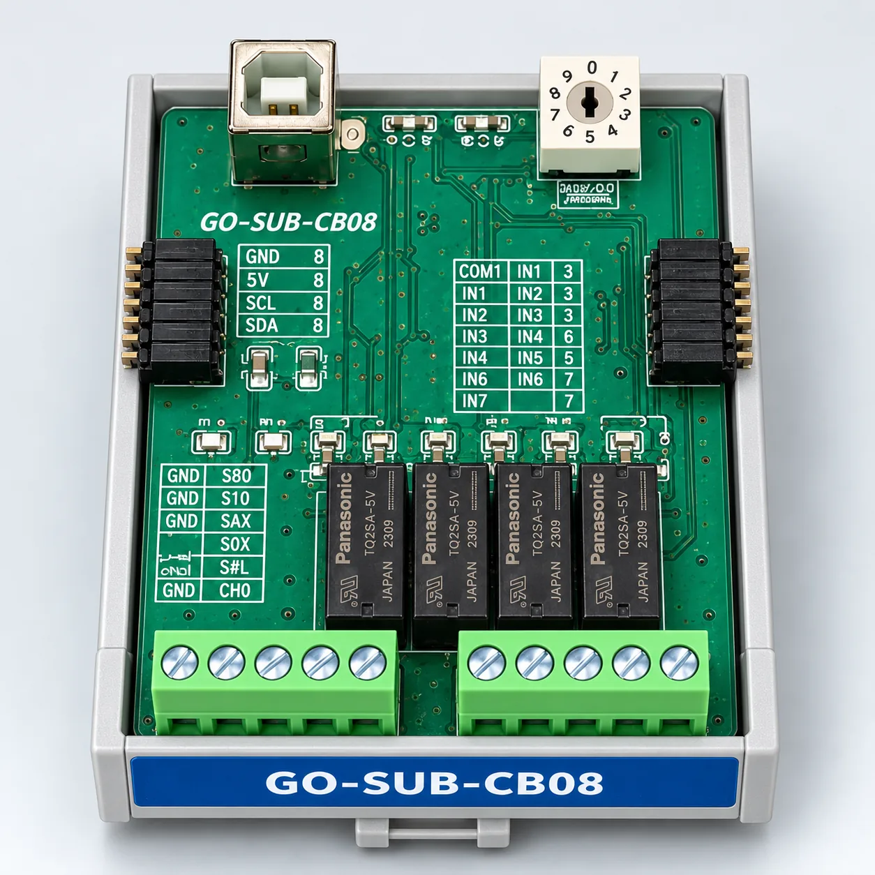
The board inside. Specifications below are from the design file.
All three share one structure
What appears identically in all three:
RP2040                     MCU
W25Q128JV                  flash
CAT811                     reset supervisor
MCP2515 + SN65HVD230       CAN controller + transceiver
LD1117S33                  3.3 V regulator
USB port + polyfuse        firmware updates
rotary switch              module address
Each module has its own MCU. The main board does not read values out of them; each module measures, decides and puts data on CAN.
Three things follow from that:
- A busy main board does not disturb the analog sampling interval
- Firmware goes on per module over USB. Changing AD04 leaves CB08 untouched
- A new module only needs this structure and the 16-pin bus to drop into an existing system
GO-SUB-CB08 — 4 relay outputs + 4 isolated inputs
The contact module.
| Function block | Part | Qty |
|---|---|---|
| Relay output | PA1A-24V | 4 |
| Relay drive | 2N3904 | 4 |
| Isolated input | KPC18T1 optocoupler | 4 |
| Surge protection | TVS P6KE8.2CA | 8 |
| Terminal block | 5-pin | 2 |
Every input passes through an optocoupler, so field contacts are electrically separated from the board logic and whatever supply the field side uses does not reach it.
The eight TVS parts are one per IO point across the four outputs and four inputs. That is also why this is the highest part count of the three, at 162.
GO-SUB-AD04 — 4 analog inputs
The measurement module.
| Function block | Part | Qty |
|---|---|---|
| ADC | MCP3428, 16-bit 4-channel | 1 |
| Input filtering | common-mode choke | 9 |
| Surge protection | TVS | 4 |
| Terminal block | 6-pin | 2 |
The function block is a single chip. What it has instead is nine chokes. On an analog input, noise becomes the reading, so the part budget went into filtering.
Fewest parts of the three at 121, and the most attention paid to the input stage.
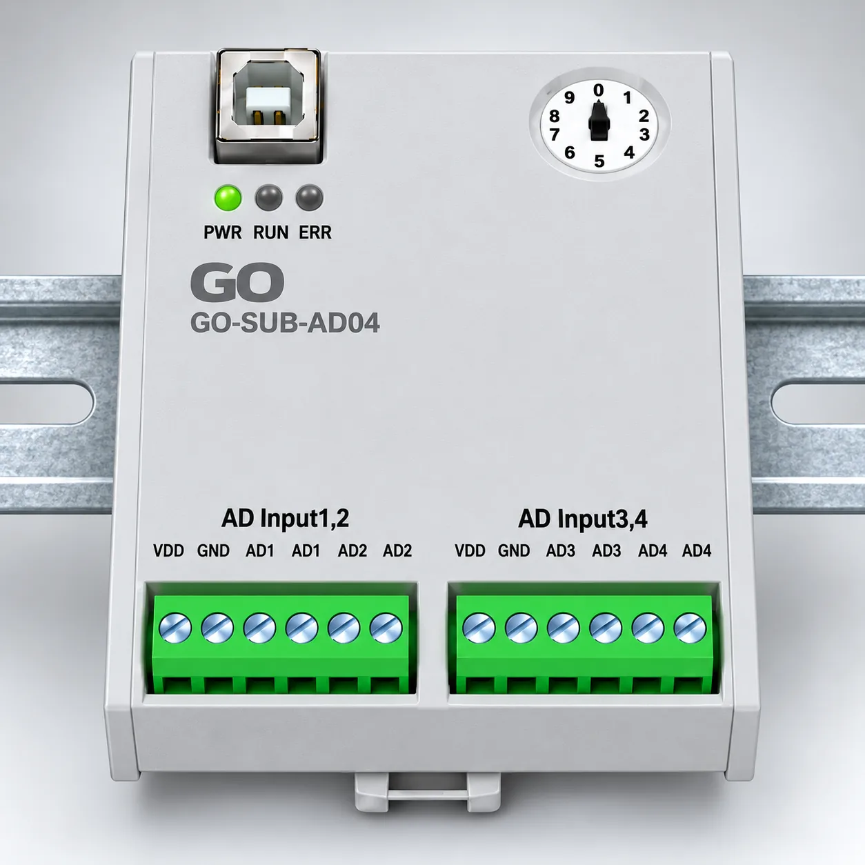
The front carries two blocks, AD Input1,2 and AD Input3,4. Each channel has two
terminals, with VDD and GND on each block.
GO-SUB-DA04 — 4 analog outputs
The signal output module.
| Function block | Part | Qty |
|---|---|---|
| Output stage | LM358 op-amp | 2 (= 4 channels) |
| Drive | 2N3904 | 8 |
| Surge protection | TVS | 4 |
| Terminal block | 6-pin | 2 |
Instead of a DAC chip, the output stage is built from op-amps and transistors. Two LM358s give four channels.
It has the most resistors of the three at 68, because on an analog output the resistor ratio is the accuracy.
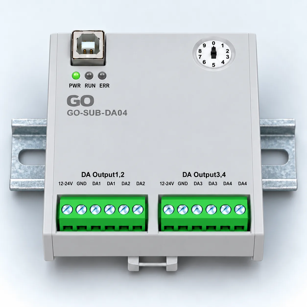
The front carries DA Output1,2 and DA Output3,4. Each block also brings out 12-24V
and GND for the output loop.
The three compared
| CB08 | AD04 | DA04 | |
|---|---|---|---|
| Function | 4 relays + 4 inputs | 4 inputs (16-bit) | 4 outputs |
| Size | 51.0 × 81.5 mm | 51.0 × 81.5 mm | 51.0 × 81.5 mm |
| Layers | 4 | 4 | 4 |
| Parts | 162 | 121 | 135 |
| Nets | 112 | 91 | 95 |
| Resistors | 77 | 59 | 68 |
| Capacitors | 27 | 27 | 31 |
| Terminals | 5-pin ×2 | 6-pin ×2 | 6-pin ×2 |
The capacitor counts — 27, 27, 31 — are nearly the same. Decoupling follows the shared structure, resistors follow the function block.
What the approach costs
An MCU and a CAN chip on every module raise the unit cost. Hanging an I2C expander off the bus would be far cheaper.
In return the modules run independently, firmware is managed per module, and adding a new module is straightforward. Never having to redesign the whole system to add channels is what this structure buys.
Part 4 collects the specifications for all four modules and covers expansion.
🔧 GO Modular IO series: Part 1 — the system · Part 2 — the main module · Part 3 — the three sub-modules · Part 4 — specs and expansion
Contact
- Email: [email protected]
- Instagram: https://www.instagram.com/going.sen/
- Website: https://intosen.com/kr/consult/
Comments
Enter a nickname to leave a comment, or sign in with Google or GitHub.